MSquare IP
Filter
Compare
10
IP
from
1
vendors
(1
-
10)
-
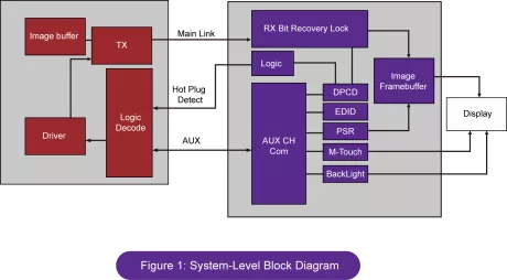
eDP PHY
- Compatible with embedded display port v1.5/v1.4b specification
- Four-lane main link with support for 8.1/5.4/4.32/3.24/2.7/2.43/2.16/1.62Gbps
- Supports Enhanced Framing Mode
- Automatic Link-Training with an option for firmware-controlled Link-Training procedure
-
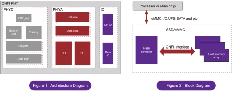
ONFI 5.1 PHY IP
- Compliant with ONFI 5.1 specification
- Supports NV-DDR3/NV-LPDDR4, with a maximum rate up to 3600MT/s
- Supports matched or unmatched DQS
- Supports WDCA/Per-Pin VREFQ Training for NAND devices
-
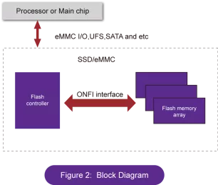
ONFI 5.0 PHY IP
- Compliant with ONFI 5.0 specification
- Supports NV-DDR2 mode
- Supports NV-DDR3, NV-LPDDR4, with a maximum rate of 2400MT/s
- Supports PHY Independent TX/RX Training mode
-
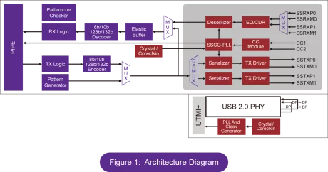
USB 3.2 Gen2x2 with PIPE 4.3 and USB2.0 with UTMI+ interface
- Fully compliant with USB 3.2 Gen2x1 featuring PIPE 4.3 and USB 2.0 with a UTMI+ interface
- Supports host, peripheral, and dual-role applications
- Supports 10/12/25/30/19.2/24/27/40 MHz crystal oscillators or clock inputs
- Supports TX 3-Tap FFE and RX CTLE+1-Tap DFE for SS+
-
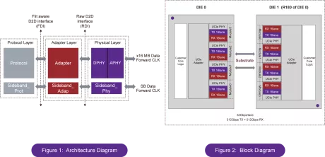
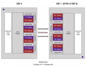
D2D UCIe 1.1
- Compatible with UCIe v1.1 specification
- Features single-ended, source-synchronous, and DDR I/O signaling
- Supports 32-bit (16-bits TX + 16-bit RX) data bus per module for standard packages
- Offers a high clock frequency up to 16GHz
-
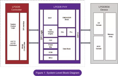
LPDDR5X PHY
- Compatible with JEDEC standards LPDDR4X , LPDDR5 and LPDDR5X SDRAMs
- Supports for data transfer rate up to 8533Mbps
- DFI 5.0 for PHY and controller interfaces
- Supports both firmware-based training and hardware-based training
-
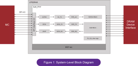
LPDDR4X PHY
- Compatible with LPDDR4X, with a maximum rate up to 4267Mbps
- Compliant with DFI 4.0 for PHY and control interfaces
- Flexible channel architecture
- Supports PHY-independent training mode using an embedded processor
-
D2D UCIe 1.0
- Compatible with UCIe v1.0 specification
- Single-ended, source synchronous and DDR IO Signaling
- Supports 32 bits(16bits TX + 16bits RX) data bus per module for standard package
- High clock frequency, up to 8GHz
-
HBM3 PHY and Controller.
- Designed for high memory throughput and low latency applications
- Consists PHY and Memory Controller
- Optimized for 12nm process
- Supports speed up to 6.4Gbps/pin
-
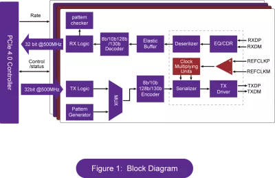
PCI Express 4.0 PHY
- Compiles with PCIe 4.0, 3.1, 2.1, 1.1 and PIPE 4.4.1 specifications
- Supports all power-saving modes (P0, P0s, P1, P2) as defined in PIPE 4.4.1 specifications
- Supports L1 PM/CPM substates with CLKREQ#
- Supports the separate REFCLK Independent SSC (SRIS) architecture