HPC IP
Filter
Compare
514
IP
from
38
vendors
(1
-
10)
-
HPC MACsec Security Modules for Ethernet
- IEEE 802.1ae, IEEE 802.1br Support
- 100 Gbps—1.6 Tbps
- Can reach higher throughputs scalable to 3.2 Tbps
- Supports also lower performance modes down to 10 Gbps
-
3.3V Capable GPIO on TSMC 28nm RF HPC+
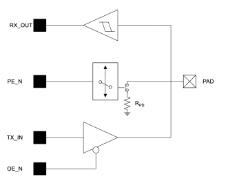
- The 3.3V capable GPIO is an IP macro for on-chip integration. It is a 3.3V general purpose I/O built with a stack of 1.8V thick oxide MOS devices. It is controlled by 0.9V (core) signals.
- Supported features include core isolation, output enable and pull enable. Extra features such as input enable/disable, programmable drive strength and pull select, can be supported upon request.

-
1.2V Thin Oxide GPIO on TSMC 28nm RF HPC+
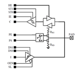
- The 1.2V Thin Gate GPIO is an IP macro for on-chip integration. It is a 1.2V general purpose I/O that does not rely on thick-gate devices. Only thin-gate, 0.9V capable core MOS devices are used in the design.
- Supported features include core isolation, programmable slew rate compensation, programmable drive strength, input/output enable, pull select and pull enable. Extra features such as programmable hysteresis can be supported upon request.

-
11-bit SAR ADC - TSMC 28nm HPC+
- The A11B4G is a low-power, high-speed analog to digital converter (ADC) intellectual property (IP) design block.
- It is a hybrid successive approximation register (SAR) ADC, with a 11-bit resolution, and a sampling speed of 4 gigasamples per second (GSPS).
-
14-bit, 200 MSPS DAC - TSMC 28 HPC+
- The D14B200M-TS28H is an ultra low-power, high-speed digital to analog converter (DAC) intellectual property (IP) block.
- It is a current steering DAC that has a 14-bit resolution, and a sampling speed of 200 megasamples per second (MSPS).
-
MIPI C/D-PHY Combo Rx IP, Silicon Proven in TSMC 28 HPC+
- Compliant with MIPI D-PHY spec up to v2.5 and C-PHY spec up to v2.0
- Support both MIPI DSI and CSI-2 protocols
- Support HS data rate up to 6Gbps ( 6Gsps ) per lane (per trio)
- Support LS data rate of 10Mbps and Ultra-low power mode

-
MIPI C/D-PHY Combo Tx IP, Silicon Proven in TSMC 28 HPC+
- Compliant with MIPI D-PHY spec up to v2.5 and C-PHY spec up to v2.0
- Support both MIPI DSI and CSI-2 protocols
- Support HS data rate up to 6Gbps ( 6Gsps ) per lane (per trio)
- Support LS data rate of 10Mbps and Ultra-low power mode

-
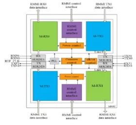
MIPI M-PHY v4.1 IP, Silicon Proven in TSMC 28 HPC+
- RX:DFE+CTLE, TX:2-tap FFE
- Max. Channel Loss:~14dB @6GHz Nyquist
- Low operation current and low standby current

-
Camera Combo Receiver - 2.5Gbps 8-Lane - TSMC 28nm HPC
- The CL12832M8R2JM3QIP2500 is an ideal means to link Camera Modules or CMOS Image Sensor (CIS) to ISP (Imaging Signal Processer) and DSP.
- The CL12832M8R2JM3QIP2500 is designed to support data rate in excess of maximum 2.5Gbps utilizing SLVS-EC / MIPI D-PHY v-1.2/ CMOS 1.8V interface specification.