DDR4 IP
Filter
Compare
223
IP
from
32
vendors
(1
-
10)
-
DDR4 IO for memory PHY, 3200Mbps on SMIC 40nm
- The DDR4 IO is used to transfer the Command/Address/Clk and Data between the memory controller PHY and the DRAM device
- The TX is designed to send information from PHY to DRAM and RX is designed to receive information which is from DRAM.
-
DDR5 & DDR4 COMBO IO for memory controller PHY, 4800Mbps on TSMC 12nm
- The DDR5&DDR4 COMBO IO is used to transfer the Command/Address/Clk and Data between the memory controller PHY and the DRAM device
- The TX is designed to send information from PHY to DRAM and RX is designed to receive information which is from DRAM._x000D_ It supports DDR5&DDR4 interface
- The DDR5 DQ data rate can be up to 4800Mb/s, and the DDR4 DQ data rate can be up to 3200Mb/s and CA is SDR mode.
-
DDR4 & LPDDR4 COMBO IO for memory controller PHY, 3200Mbps on TSMC 22nm
- The DDR4&LPDDR4 COMBO IO is used to transfer the Command/Address/Clk and Data between the memory controller PHY and the DRAM device
- The TX is designed to send information from PHY to DRAM and RX is designed to receive information which is from DRAM.
-
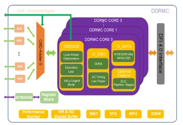
DDR3 and DDR4 Controller and PHY on TSMC 12nm
- This DDR3/4 IP combo solution presented, is meticulously designed for high performance and low power consumption, utilizing sophisticated architecture and advanced technology.
- Fabricated in TSMC’s 12nm CMOS process, this solution includes both controller and PHY IPs, providing comprehensive support for DDR3 and DDR4 memory interfaces.
-
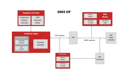
DDR4 Controller - Validates memory compliance, optimizes performance, ensures reliability
- The DDR4 Memory Controller Verification IP ensures compliance with DDR4 standards, validating high-speed data transfer, read/write operations, and error correction. It provides automated testing, advanced debugging tools, and scalability for complex memory systems.
- Designed for versatile applications, this IP optimizes performance in gaming consoles, data centers, AI systems, networking devices, and more. It ensures memory reliability, efficiency, and scalability across industries, accelerating time-to-market for DDR4-based products
-
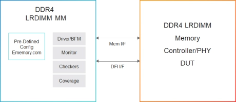
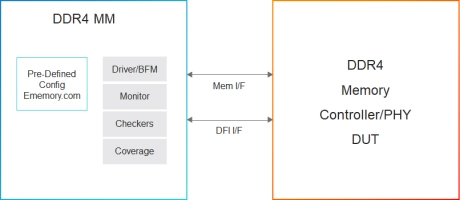
Simulation VIP for DDR4 LRDIMM
- DIMM Types
- DDR4 UDIMM, RDIMM, LRDIMM, DDR4 3DS, 3DS UDIMM, 3DS RDIMM, and 3DS LRDIMM
- LRDIMM Training Modes
- Fully supports DWL, HWL, MREP, MRD, and MWD Training modes
-
Simulation VIP for DDR4
- Data Width, Density
- 4, 8, and 16. 2 Gb to 16 Gb
- Speed
- 1600, 1866, 2133, 2400, 2666, and 3200
-
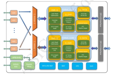
DDR4 IP solution
- Compatible with DDR4 up to 3200Mbps
- AXI compliant multi-ports, and data width, FIFO depth, command queue depth configurable
- DFI compliant interface between controller and PHY
- Support ECC (error correcting code)
-
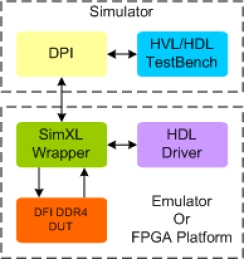
DDR4 DFI Synthesizable Transactor
- Compliant with DFI version 3.0 or higher Specifications.
- DFI-DDR4 Applies to :
- DDR4 protocol standard JESD79-4, JESD79-4A, JESD79-4A_r2,JESD79-4B, JESD79-4C and JESD79-4D (draft) Specification
- Supports all Interface Groups.
-
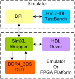
DDR4 3DS Synthesizable Transactor
- Supports 100% of DDR4 3DS protocol standard JESD79-4-1, JESD79-4-1A and JESD79-4-1B
- Supports all the DDR4 3DS commands as per the specs
- Supports up to 16 GB device density
- Supports X4 and X8 devices types