Baseband IP
Filter
Compare
391
IP
from
58
vendors
(1
-
10)
-
Bluetooth Dual Mode v5.3 Baseband Controller IP
- Software Memory footprint (ARM Cortex M0/M3): ROM ~ 300KB ; RAM ~ 112 KB
- Combined Hardware gate count : 250 k gates
- Arbitration logic implemented in hardware and assisted by software
- Baseband and LE LL Accelerator
-
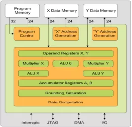
Baseband processor
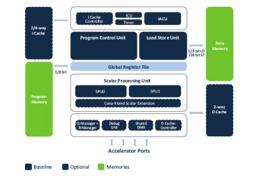
- The Ceva-BX2 baseband processor IP handles both signal-processing and control workloads with up to 16 GMACs per second performance and high-level-language programming.
- It supports a range of integer and floating-point data types for a wide range of baseband applications like 5G PHY control, and exploits a high degree of parallelism, but with remarkably compact code size.
- Optimized high-speed interfaces expedite connection to other Ceva cores or to accelerators.
-
Dual band WiFi N/G/B/A Digital Baseband IP
- Supports data rates upto 65Mbps
- Throughput numbers of above 50 Mbps for UDP and above 40 Mbps for TCP.
- Support for authentication methods (Cisco® LEAP, PEAP with EAP-GTC support, CCKM with EAP-FAST) depend on the host platform.
- Supports MAC enhancements including:802.11d -Regulatory domain operation,802.11e -QoSincluding WMM,802.11h –Transmit power control dynamic and frequency selection,802.11i -Security including WPA2 and WAPI compliance,802.11k -Radio resource measurement,802.11r –Roaming,802.11w -Management frame protection
-
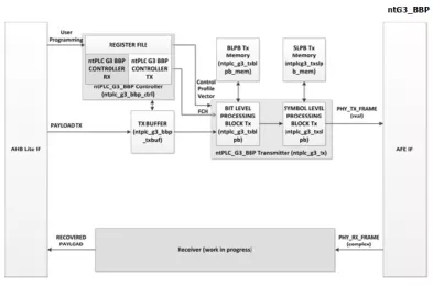
Smart Grid PLC Baseband Processor
- PLC G3 physical layer (PHY) compliant baseband processor as per ITU-T G.9903 Chapter 7 and ITU-T G.9901 Annex B.
-
SMIC 65nm LL Small signal digital clock buffer for baseband application
- Small signal digital clock buffer for baseband application;
- Cell Size (Width * height)90um * 180um with DUP stagger bonding pads;
- Work voltage: 1.2V power;
- Support >600mV clock signal input;Support 0.3V~0.5V wide input offset voltage range;
-
-
OFDM Baseband Processor
- Customized transmit and receive physical layer chains.
- Fully synchronous design enabling high throughput TDD operation.
-
Ultra low power C-programmable Baseband Signal Processor core
- Ultra low power consumption
- Highly optimizing C-compiler software toolkit
- Minimal core size (65k gates), excluding debug interface (6k gates)
- Small memory footprint
-
Licensable baseband controller core + Licensable upper and lower protocol stacks
- BLUETOOTH
- LICENSABLE IP
-
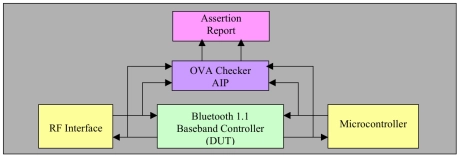
Bluetooth Baseband Controller OVA Checker IP
- Fully compliant with Bluetooth Specifications Ver 1.1 as specified by Special Interest Group (SIG).
- Compliance to Test Suites as provided Standard Sample Test from Bluetooth Qualification Body (BQB).
- Reduced Area by logical sharing thereby Low Power Consumption.
- Time Division Duplex (TDD).