BIST IP
Filter
Compare
865
IP
from
51
vendors
(1
-
10)
-
eFlash BIST IP
- The BIST can realize all eFlash testing items, covering UMC’s 40nm and 55nm processes, as well as SST’s 0.11um and 0.18um processes, and customized embedded eFlash IP wafer software testing and final testing.
- The BIST features a flexible serial interface, reducing the need for IC test pins and increasing testing flexibility.
-
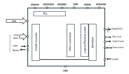
UCIe TX Interface
- Transmit-only UCIe REV1.1 with FIFO Interface
- TSMC 16FFC process
- Low power UCIe D2D
- 1 pJ/bit at 0.7V
-
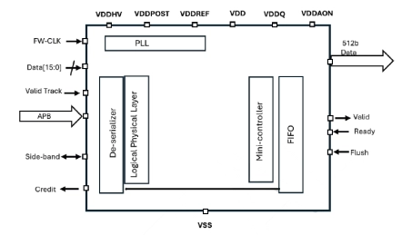
UCIe RX Interface
- Receive-only UCIe Rev1.1 with FIFO Interface
- Samsung 8nm process
- Low power UCIe D2D
- 1 pJ/bit at 0.7V
-
HPC MACsec Security Modules for Ethernet
- IEEE 802.1ae, IEEE 802.1br Support
- 100 Gbps—1.6 Tbps
- Can reach higher throughputs scalable to 3.2 Tbps
- Supports also lower performance modes down to 10 Gbps
-
UALinkSec Security Module
- UALink 200 v1.0 / UALinkSec specification support
- Plug and play with Synopsys UALink controller
- Supports 200 GT/s per lane, enabled by silicon-proven Synopsys 224G PHY IP
- Support bifurcation of up to 4 ports
-
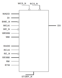
Dual Port Register File Compiler (1 Read-only port, 1 Write-only port) - GF 22FDX+
- Uses 8T-TP185SL bit cells.
- Isolated Supplies: Periphery and array power domains can be independently powered down in standby mode.
- Deep Sleep Standby Mode: Memory retains data at minimal power via internal biasing.
-
HBM4 PHY IP
- Supports JEDEC HBM4 DRAMs
- Supports data rates up to 12 Gbps
- Supports up to 32 independent 64-bit memory channels
- Pseudo-channel operation supported to enable up to 64 32-bit pseudo-channels with 2048-bit PHY
-
USB Super-speed+ PHY
- Fully compliant with USB 3.2 Gen2 specification.
- Supports data rates of 5Gbps (Gen1), 10Gbps (Gen2), and 20Gbps (Gen2x2).
- Compatible with PIPE interface:
- 8/16/32-bit at original PIPE.
-
SLVS-EC RX PHY IP
- Fully compliant with SLVS-EC v3.0 specification.
- Supports both synchronous and asynchronous clocking.
- Up to 10Gbps per lane with 40-bit parallel data bus.
- Maximum output clock frequency of 250MHz.