SD/eMMC PHY, SDIO, eMMC IO for SMIC
Welcome to the ultimate
SD/eMMC PHY, SDIO, eMMC IO
for
SMIC
hub! Explore our vast directory of
SD/eMMC PHY, SDIO, eMMC IO
for
SMIC
All offers in
SD/eMMC PHY, SDIO, eMMC IO
for
SMIC
Filter
Compare
15
SD/eMMC PHY, SDIO, eMMC IO
for
SMIC
from
7
vendors
(1
-
10)
-
LVDS Deserializer IP
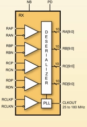
- The MXL-DS-LVDS is a high performance 4-channel LVDS Deserializer implemented using digital CMOS technology.
- Both the serial and parallel data are organized into four channels. The parallel data can be 7 or 10 bits wide per channel. The input clock is 25MHz to 165MHz. The De-serializer is highly integrated and requires no external components.
-
LVDS Serializer IP
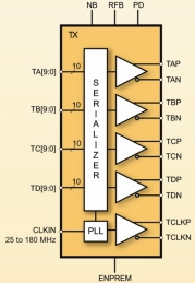
- The MXL-SR-LVDS is a high performance 4-channel LVDS Serializer implemented using digital CMOS technology. Both the serial and parallel data are organized into four channels.
- The parallel data width is programmable, and the input clock is 25MHz to 165MHz. The Serializer is highly integrated and requires no external components.
-
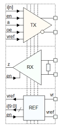
LVDS Transceiver
- Meets or exceeds the TIA/EIA-644 LVDS standard.
- Driver, Receiver, Bias, and Power cells included.
- Greater than 400Mbs data rate.
- 1.8V core voltage, 5V IO voltage.
- Receive fault detection.
- 0.3ns differential pulse skew.
-
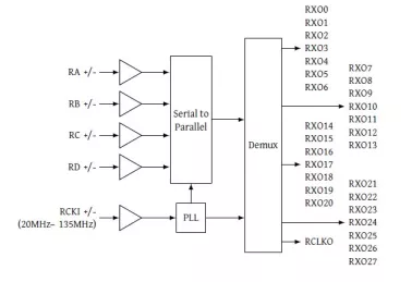
LVDS Receiver PHY
- Converts 5-pair LVDS data stream into parallel 35 bits of CMOS data
- Compatible with the TIA/EIA-644 LVDS standards
- Supports up to 1.05Gbps data rate for UXGA
- On-chip DLL requires no external component
-
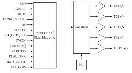
LVDS transmitter PHY
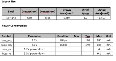
- Silicon Proven in 22,28,55,65,130n,180n from SMIC, Global Foundries and Samsung
- Compatible with the National DS90CF386
- Compatible with the TIA/EIA-644 standards
- Converts 35 bits data to 5-pair LVDS data stream
-
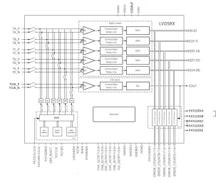
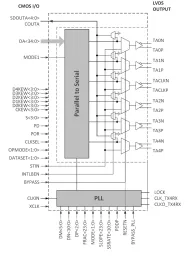
V-by-One Tx IP, Silicon Proven in SMIC 40LL
- 16 channels total 128 bits of parallel data, each channel has a bit width of 8 bits
- DC coupling mode
- Multi-channel shared offset
- Built-in transmitter terminal impedance, no need for off-chip components
-
LVDS Receiver
- Wide frequency range:
- Power-Down Mode
- Supports VGA, SVGA, XGA, SXGA, SXGA+ and QXGA
- Up to 10.5 Gbit/s bandwidth
-
LVDS Transmitter
- Wide frequency range:
- Power-Down Mode
- Supports VGA, SVGA, XGA, SXGA, SXGA+ and QXGA
- On-chip Input Jitter Filtering
-
subLVDS I/O Pad Set
- Input receive sensitivity of 50mV peak differential (without hysteresis)
- Common mode range from 0.4V to 1.6V (limited by Power Supply)
- Powered by 1.8V I/O and 1.1V core supplies
- Power consumption: 3.4 mW max @ 800 MHz
-
Mini LVDS Transmitter
- Selectable dual operation modes:
- Output offset voltage selectable from 0.8 – 1.5 V
- Output swing selectable from 200 – 500 mV
- Pre-emphasis selectable from 0 – 6 dB