The NAND flash controller IP provides easy, reliable access to an off-chip NAND flash. It supports all modes of the Open NAND Flash Interface (ONFI) Specification, revision 5.0, release candidate 0.5, dated 1 March 2021. It is backwards compatible, supporting the Single Data Rate (asynchronous) mode, the double data rate moves NV-DDR, NV-DDR2, and NVDDR3, to include the latest NV-LPDDR4 recently introduced in the latest revision. All posted rates for these various modes are also supported, from the NV-DDR 33MHz mode at the low end all the way up to the newer 1,200MHz (2.4GT/s) I/O speeds.
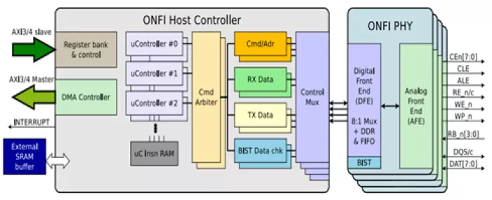
The IP consists of two primary components: a host controller and two or more high speed PHY interface controllers. The host controller is controlled via an AXI slave port. A scatter/gather DMA provides a separate AXI master port, allowing for extended unattended reads or writes. The host controller supports either AXI3 or AXI4, and a user configurable data path width.