The ONFI 3.2 compliant NAND Flash Controller IP Core is a full featured, easy to use, synthesizable design that is easily integrated into any SoC or FPGA development. Designed to support both SLC and MLC flash memories, it is flexible in use and easy in implementation. The controller works with any suitable memory device up to 128 Gb from leading memory providers such as Micron, Samsung, Toshiba, Hynix, and others.
The ONFI 3.2 NAND Flash Controller IP core includes a host of configuration options from page size to band selects. The controller offers Hamming Code (1bit error correction and 2bit error detection) and Arasan’s patent pending BCH (option for 4-, 8-, 12- and 64-bit error correction or more.) error code correction (ECC) for optimized performance and reliability. Additional features include the capability to boot from flash. The IP core supports the Open NAND Flash Interface Working Group (ONFI) 3.1 standard and is backwards compatible. It uses differential signaling on the clock and data lines and clocks at any frequency up to 200 MHz.
ONFI 3.2 NAND Flash controller supports a variety of host bus interfaces for easy adoption into any design architecture. An optional ONFI software stack and driver for Linux is available to shorten engineers’ development time and efforts features.
ONFI 3.1 improves on version ONFI 3.0 with more robust power sequencing to protect NAND flash, more flexible timing to support NAND usage in different topologies, improved parameters for testing, and other enhancements.
Supports ONFI 3.2 and backward compatible to ONFI 3.0, 2.3, 1.0
Supports Toggle DDR-2 and asynchronous SDR
Upto 533 MT/s high performance with patent pending ECC engine with code-length configurable BCH coder and decoder
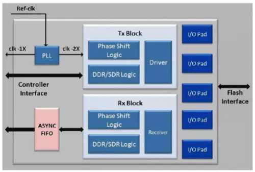
Proven and robust high performance ONFI 3.2 NV-DDR2 PHY delivered in RTL with synthesizable DLL/PLL
I/O pads compatible to ONFI 3.2 266Mhz NV-DDR2 operation at 1.8v or 3.3v
Optionally, a hardened ONFI 3.2 PHY delivered in GDSII including DLL and PLL is avaible
Offered as a Total IP solution including RTL Host Controller IP, Verification IP, Software Stack, and Hardware Development Platform