The Arasan ONFI 2.3 NAND Flash Controller IP Core is a full featured, easy to use, synthesizable core, easily integrated into any SoC or FPGA development. Designed to support both SLC and MLC flash memories, ONFI 2.3 NAND controller IP is flexible in use and easy in implementation. The controller works with any suitable NAND Flash memory device up to 128 Gb from leading memory providers – Micron, Samsung, Toshiba and Hynix. The IP core includes a host of configuration options from page size to band selects. The controller offers Hamming Code (1-Bit error correction and 2-Bit error detection) and BCH (option for 4-, 8-, 12-, up to 32-Bit error correction) error code correction (ECC) for optimized performance and reliability. Additional features include the capability to boot from flash.
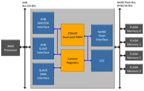
This NAND Controller IP core supports the Open NAND Flash Interface Working Group (ONFI) 1.0, 2.0, 2.1, 2.2 and 2.3 standards and the Micron ClearNAND. It can also support a variety of host bus interfaces for easy adoption into any design architecture – AHB, APB, OCP, 8051 or custom buses. The slave AHB IP supports an external DMA interface where the master AHB incorporates an internal DMA controller.
An optional NAND Flash File system is available to support advanced features. The file system converts complicated tasks of NAND flash memory interfacing to simple memory access. Flash memory read, write, garbage collection, bad block management and other functions are handled in the background by the file system.
ONFI 2.3 NAND Flash Controller
Overview
Key Features
- Compliant to ONFI 2.3
- Supports speed ranging from 40MB/s to 200MB/s
- Supports synchronous modes
- Supports asynchronous mode [0-5]
- Supports Flash devices up to 128Gb
- Boot mode support
- Supports all mandatory commands and selected optional commands Full access to spare area
- Supports Interleaving Operations
- Supports Micron ClearNAND.
- Supports EZ – NAND devices
- Supports Micron ClearNAND
Benefits
- Fully compliant core Premier direct support from Arasan IP core designers
- Easy-to-use industry standard test environment
- Unencrypted source code allows easy implementation
- Reuse Methodology
- Manual guidelines (RMM) compliant verilog code ensured using Spyglass
Block Diagram
Deliverables
- RMM Compliant
- Synthesizable RTL design in Verilog
- Easy-to-use test environment
- Synthesis scripts Technical documents
Technical Specifications
Maturity
Silicon Proven
Availability
Now