The High Speed Synchronous Serial Interface (HSI) Controller is used to provide high bandwidth, point-to-point, serial communication between two peers, like the cellular modem and application processor on a mobile platform, such as a smartphone or a tablet. The Arasan HSI Controller IP is designed to provide MIPI HSI 1.00 compliant connectivity to a SoC.
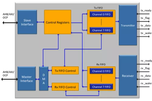
Three flavors of the IP are currently available, namely, with support for AHB, AXI or OCP system buses. The IP’s internal registers are accessible through programmed IO transactions, in which case the IP functions as a bus slave. All data transfers between the SoC’s system memory and HSI interface happen either in PIO mode or in DMA mode as programmed by the driver/firmware.
All data received from system memory is held in the transmit FIFO and output as serial data over the HSI physical interface. Conversely, all serial data received from the HSI interface is captured in the receive FIFO before it is sent to the system memory. The FIFO’s and their associated logic can be structured with up to 8 logical channels, each with configurable depth.
MIPI HSI Controller - (High-Speed Synchronous Serial Interface)
Overview
Key Features
- Compliant with MIPI HSI Specification version 1.0, and Physical Layer version 1.01.00
- Delivered in Reuse Methodology Manual (RMM) compliant Verilog RTL format
- Small footprint
- Full Duplex High Speed Serial Interface between two peer devices
- HSI clock frequency range from 1MHz to 200 MHz
- Maximum bandwidth of 200 Mbps in both Transmit and Receive directions
- Programmable transmission bit rate
- Supports 1 to 8 logical channels for both Transmit and Receive
- Configurable FIFO depth for each channel
- Runtime configuration of channel id
- Arbitration for multi-channel transmits
- Supports all three Receive data flows defined in the standard
- Synchronized, Pipelined and Real-time
- Supports Stream and Frame modes for data Transmission
- 32 bit AHB, AXI or OCP Interface to CPU/Memory sub-system
- System Clock frequency range from 30 to 200 MHz
- Master Interface used for DMA read/writes with main memory
- AXI/OCP Master supports 8 outstanding requests
- Separate Slave Interface used for register access
Benefits
- Fully compliant to MIPI standard
- Small footprint
- Code validated with Spyglass
- Functionality ensured with comprehensive verification
- Product quality proven with silicon
- Premier direct support from Arasan IP core designers
Block Diagram
Deliverables
- Verilog HDL of the IP Core
- Synthesis scripts
- Verification environment
- User guides for design and verification
Technical Specifications
Maturity
Silicon Proven
Availability
Now
Related IPs
- Synchronous Serial Interface Controller
- MIPI DSI-2 host/device controllers for high-speed serial interface between application processor and displays
- SSI (Synchronous Serial Interface) Verification IP
- Expanded Serial Peripheral Interface (xSPI)Master Controller
- Expanded Serial Peripheral Interface (xSPI) Slave Controller
- PSI5 IP Core Controller for Peripheral Sensor Interface 5 Communication