The Low Voltage Differential Signaling (LVDS) I/O library is a high-frequency interface that uses differential signals for data transmission. Typical LVDS I/O applications include displays, printers, and other high-speed data interfaces. This LVDS IP includes a transmitter, receiver, and a novel equalization design supporting programmable pre-emphasis at the transmitter. Operating at 1 GHz, this LVDS supports data transfers rates up to 2 Gbs. Including built-in termination resistors, DFT compliance, and robust ESD, this LVDS I/O delivers the most reliable performance and is silicon proven.
LVDS I/O IP - High Frequency Transceiver
Overview
Key Features
- Up to 1 GHz operation (2 Gbs)
- Novel equalization with programmable emphasis
- Compensation block provides PVT-invariance
- Built-n termination resistors
- Common mode support of both RX and TX
- 2 KV HBM ESD compliance
- Operating temperature of -40°C to 125°C•Silicon proven
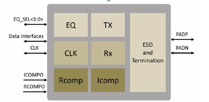
Block Diagram
Deliverables
- Models
- IBIS
- Timing
- LEF
- GDSII
- Datasheet
Technical Specifications
Short description
LVDS I/O IP - High Frequency Transceiver
Vendor
Vendor Name
Foundry, Node
Universal
Maturity
Silicon Proven
Availability
Now
Related IPs
- LVDS IO handling data rate up to 50Mbps with maximum loading 60pF
- Multi-constellation and Multi-frequency Correlators Soft GNSS IP for high sensitivity and high accuracy GNSS receivers
- High-Speed LVDS (SERDES) Transceiver
- High Channel Count DMA IP Core for PCI-Express
- GSMC 0.18um CIS process LVDS Transceiver Pad
- Bluetooth Dual Mode v4.2 RF Transceiver IP