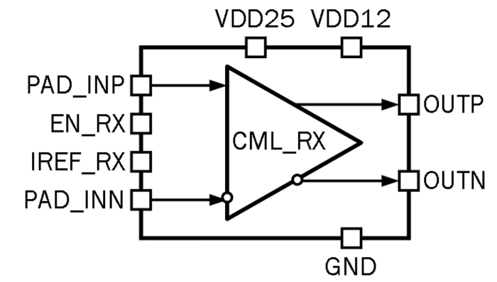
065TSMC_CML_01 core logic interface includes complementary output signal pins (OUTp, OUTn) for data transmission and enable pin EN_RX. PAD_INP and PAD_INN are differential input pins that should be connected to bonding pads. Buffer includes two 50-Ohm on-chip termination resistors, connected to supply voltage node. So the interface supports both AC and DC-coupled connections. IREF_RX is a reference current input.
3.125 Gbps DDR CML receiver
Overview
Key Features
- TSMC CMOS 0.065 um
- 1.2 V digital power supply
- 2.5 V CMOS input logic signals
- 1.2 V CMOS input logic signals
- 3.125 Gbps (DDR MODE) switching rates
- Temperature range: -40 °C to + 125 °C
- Optimized for pad-limited layout design
- Portable to other technologies (upon request)
Block Diagram
Applications
- Point-to-point data transmission
- Multidrop buses
- Clock distribution
- Backplane receiver
- Backplane data transmission
- Cable data transmission
Deliverables
- Schematic or NetList
- Abstract model (.lef and .lib files)
- Layout view (optional)
- Behavioral model (Verilog)
- Extracted view (optional)
- GDSII
- DRC, LVS, antenna report
- Test bench with saved configurations (optional)
- Documentation
Technical Specifications
Short description
3.125 Gbps DDR CML receiver
Vendor
Vendor Name
Foundry, Node
TSMC CMOS 65 nm
Maturity
silicon proven
Availability
Now
TSMC
Silicon Proven:
65nm
G