cache controller IP
Filter
Compare
195
IP
from
33
vendors
(1
-
10)
-
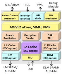
64-bit CPU Core with Level-2 Cache Controller
- AndeStar™ V5 Instruction Set Architecture (ISA), compliant to RISC-V technology
- Floating point extensions
- DSP/SIMD ISA to boost the performance of voice, audio, image and signal processing
- Andes extensions, architected for performance and functionality enhancements
- Separately licensable Andes Custom Extension™ (ACE) for customized acceleration
-
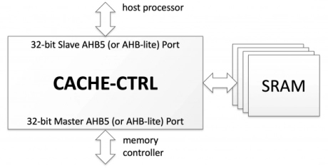
AHB Cache Controller
- The CACHE-CTRL IP core is a flexible cache memory controller providing a 32-bit slave processor interface and a 32-bit master interface to the memory subsystem. The processor and memory interfaces are natively AHB5 and can easily be reduced to AHB-lite.
- The cache controller core supports a four-way associative cache memory and implements a Least Recently Used (LRU) replacement policy.
-
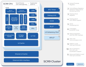
High-performance Linux-capable application core with a 12-stage dual-issue out-of-order pipeline, a VPU, cache coherency, and a hypervisor
- SCR9 is a high-performance, silicon-proven, Linux-capable 64-bit RISC-V processor core for entry-level server-class applications and personal computing devices.
- The SCR9 core supports RISC-V standard "I" Integer, "M" Integer Multiplication and Division, "A" Atomic, "C" 16-bit Compressed, "F" Single-Precision Floating-Point, "D" Double-Precision Floating-Point, "V" Vector Operations, "B" Bit Manipulation, and "K" Scalar Cryptography extensions.
-
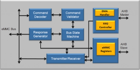
eMMC 4.51 Device Controller IP
- Compliant to JEDEC JESD84-B45 eMMC 4.51 spec
- Packed commands for faster processing
- Supports cache control mechanism
- Supports eMMC4.51 Security Protocol Commands
-
ONFI 2 NAND Flash Controller IP Compliant to JEDEC
- The ONFI 2.3 NAND Flash Controller IP Core is a full-featured, easy to use, synthesizable core, easily integrated into any SoC or FPGA development.
- Designed to support both SLC and MLC flash memories, ONFI 2.3 NAND controller IP is flexible in use and easy in implementation.

-
MIPI LLI Controller
- The LLI Controller connects two chips together to create a single “virtual chip”, with both chips sharing the same memory.
- This is achieved by the low latency from the “companion” chip to the memory interface of the host chip.
-
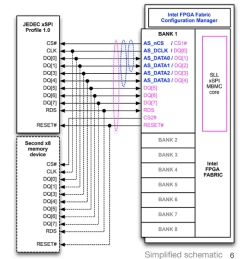
xSPI Multiple Bus Memory Controller
- SLL’s unified xSPI Multiple Bus Memory Controller IP supports the widest range of JEDEC xSPI and xSPI-like NOR Flash and PSRAM memories (JEDEC xSPI Profile 1.0 and 2.0, HyperBus 1.0, 2.0 and 3.0, OctaBus and Xccela Bus) that are available now from many memory vendors.
- JEDEC xSPI and xSPI-like memories offer good performance with lower hardware and power costs. Memory device variants offer up to 512 Mbit PSRAM, up to 2 Gigabit NOR Flash, up to 250 MHz DDR clock speeds, with x4, x8 and x16 data path widths, and a wide range of package options including 4mm x 4mm BGA49 and tiny WLCSP footprints. Some PRSAM devices are now also available with internal ECC.
-
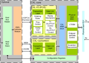
CXL CONTROLLER IIP
- Compliant with CXL 1.0/1.1 Specifications
- Supports Native PCIe mode and below features as defined in the PCIe specification
- PCIE Express specs 1.0/2.0/3.0/4.0/5.0
- PIPE interface
-
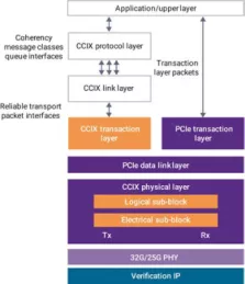
CCIX 32G Premium Controller with AMBA bridge II
- Supports all required features of the CCIX 1.1 specification, including 32GT/s, and ESM support for 25GT/s and 20GT/s
- Supports all required features of the PCIe 4.0 (16 GT/s), 3.1 (8 GT/s), 2.1 (5 GT/s), 1.1 (2.5 GT/s) and PIPE (8-, 16- and 32-bit) specifications
- Choice of datapath widths (128-bit, 256-bit, or 512-bit)
- Supports cache-coherency as defined by the CCIX standard