PHY IP
Filter
Compare
3,766
IP
from
200
vendors
(1
-
10)
-
Universal Chiplet Interconnect Express PHY IP - GLOBALFOUNDRIES® 22FDX®
- Delivered as Hardmacro IP
- Implementation of the physical layer of the UCIe standard from Raw D2D Interface (RDI) to electrical interface of UCIe main band (MB) and sideband (SB)
- Includes TX and RX side
-
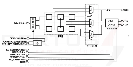
32Gbps SerDes PHY in GF 22nm
- This 32Gbps SerDes PHY is implemented in GlobalFoundries 22FDX CMOS technology and provides a high-performance, protocol-agnostic serial interface for advanced mixed-signal and high-speed digital SoCs.
- The PHY is architected as a modular design consisting of a low-jitter clock multiplier, a half-rate transmitter with digitally programmable feed-forward equalization, and a configurable CTLE-based receiver with digital clock-and-data recovery, supporting both 16 Gbps and 32 Gbps operation.
-
HBM4 PHY IP
- Supports JEDEC HBM4 DRAMs
- Supports data rates up to 12 Gbps
- Supports up to 32 independent 64-bit memory channels
- Pseudo-channel operation supported to enable up to 64 32-bit pseudo-channels with 2048-bit PHY
-
USB Super-speed+ PHY
- Fully compliant with USB 3.2 Gen2 specification.
- Supports data rates of 5Gbps (Gen1), 10Gbps (Gen2), and 20Gbps (Gen2x2).
- Compatible with PIPE interface:
- 8/16/32-bit at original PIPE.
-
SLVS-EC RX PHY IP
- Fully compliant with SLVS-EC v3.0 specification.
- Supports both synchronous and asynchronous clocking.
- Up to 10Gbps per lane with 40-bit parallel data bus.
- Maximum output clock frequency of 250MHz.
-
UCIe PHY (Die-to-Die) IP
- Compliant with UCIe v2.0, supporting 4/8/12/16/24/32GT/s data rates
- for Standard Package up to 16 lanes / for Advanced Package up to 64 lanes
- Provides a 1024-bit data bus width with high-throughput die-to-die communication
- Includes automatic per-lane calibration and optional transmitter de-emphasis
-
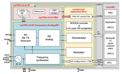
Bluetooth® Low Energy 6.2 PHY IP with Channel Sounding
- The icyTRX-LE-22 RF transceiver PHY IP delivers an optimal trade-off between power consumption and Bluetooth Low Energy (LE) RF performance — excellent sensitivity and strong interference rejection — while minimizing the overall cost for loT applications.
- Occupying just 0.57 mm2 in a 22 nm technology (7 metal layers), the analog RF portion of the IP integrates on-chip passives and Built-In-Self-Test (BIST) structures to drive down silicon area, wafer cost, bill of materials, and production-test expenses.
-
LPDDR6/5X/5 PHY V2 - TSMC N6
- The LPDDR6/5X/5 PHY IP enables ASICs, ASSPs, system-on-chips (SoCs), and system-in-package applications requiring high-performance LPDDR6, LPDDR5X, and/or LPDDR5 SDRAM interfaces operating at up to 14.4 Gbps
- With flexible configuration options, the LPDDR6/5X/5 PHY IP can be used in a variety of applications supporting LPDDR6, LPDDR5X, and/or LPDDR5 SDRAMs, precisely targeting the specific power, performance, and area (PPA) requirements of these systems
- LPDDR6 SDRAM’s combination of high bandwidth, capacity, low power, and cost effectiveness makes LPDDR6/5X/5 SDRAMs an attractive solution for traditional and new markets
- The LPDDR6/5X/5 PHY IP is designed to appeal to a variety of applications including: * Traditional mobile environments * Consumer products * Automotive solutions * Artificial intelligence * Data center applications

-
LPDDR6/5X/5 PHY V2 - TSMC N5A for Automotive, ASIL B Random, AEC-Q100 Grade 2
- The LPDDR6/5X/5 PHY IP enables ASICs, ASSPs, system-on-chips (SoCs), and system-in-package applications requiring high-performance LPDDR6, LPDDR5X, and/or LPDDR5 SDRAM interfaces operating at up to 14.4 Gbps
- With flexible configuration options, the LPDDR6/5X/5 PHY IP can be used in a variety of applications supporting LPDDR6, LPDDR5X, and/or LPDDR5 SDRAMs, precisely targeting the specific power, performance, and area (PPA) requirements of these systems
- LPDDR6 SDRAM’s combination of high bandwidth, capacity, low power, and cost effectiveness makes LPDDR6/5X/5 SDRAMs an attractive solution for traditional and new markets
- The LPDDR6/5X/5 PHY IP is designed to appeal to a variety of applications including: * Traditional mobile environments * Consumer products * Automotive solutions * Artificial intelligence * Data center applications

-
LPDDR6/5X/5 PHY V2 - TSMC N5
- The LPDDR6/5X/5 PHY IP enables ASICs, ASSPs, system-on-chips (SoCs), and system-in-package applications requiring high-performance LPDDR6, LPDDR5X, and/or LPDDR5 SDRAM interfaces operating at up to 14.4 Gbps
- With flexible configuration options, the LPDDR6/5X/5 PHY IP can be used in a variety of applications supporting LPDDR6, LPDDR5X, and/or LPDDR5 SDRAMs, precisely targeting the specific power, performance, and area (PPA) requirements of these systems
- LPDDR6 SDRAM’s combination of high bandwidth, capacity, low power, and cost effectiveness makes LPDDR6/5X/5 SDRAMs an attractive solution for traditional and new markets
- The LPDDR6/5X/5 PHY IP is designed to appeal to a variety of applications including: * Traditional mobile environments * Consumer products * Automotive solutions * Artificial intelligence * Data center applications
