ONFI 4.0 NAND Flash IP
Filter
Compare
4
IP
from
3
vendors
(1
-
4)
-
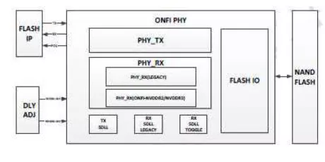
ONFi PHY 4.0 (FPHY+MDLL+SDLL Regulator) (Silicon Proven in TSMC 28HPC+)
- Support ONFi 4.0 IO Electrical Specification
- Support Legacy up to 50MHz
- Support NV-DDR2 with operating frequency up to 533Mbps
- Support NV-DDR3 with operating frequency up to 800Mbps
-
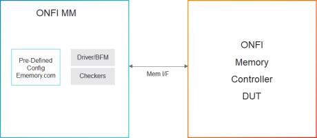
Simulation VIP for ONFi
- Hundreds of protocol and timing checkers to easily catch design bugs
- Hundreds of predefined configurations based on specific memory vendors' part numbers, datasheets, or generic JEDEC definitions available on ememory.com(opens in a new tab)
- Transaction and memory callbacks for all protocol, model states and device memory events
-
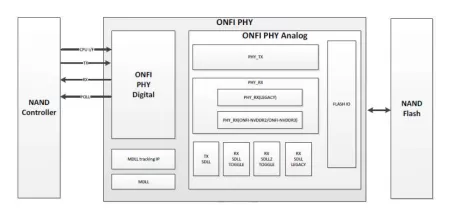
ONFI 4.1 PHY IP (Silicon Proven in TSMC 12FFC)
- Support ONFi 4.1 IO Electrical Specification
- Support Legacy up to 50MHz
- Support NV-DDR2 up to 533Mbps
- Support NV-DDR3 up to 1200Mbps
-
Advanced Flash Controller Interface Core
- Multi-Port Architecture allows connecting up to 32 NAND devices (128 total NAND targets)
- Separate Administrative and I/O queues for flexible datapath management
- Maximum of 1 register write per command submission/ completion
- Industry standard bus interface (AXI-4) master used for command fetching, command completion, and data movement