FinFET IP
Filter
Compare
731
IP
from
25
vendors
(1
-
10)
-
Current Output 12-bit 3.6GSPS RF DAC on 16nm FinFET
- The ODT-DAC-12B3P6G-16 is a high performance current steering 12-bit DAC that operates at an update rate of up to 3.6GSPS. The DAC uses a proprietary architecture that reduces harmonic and intermodulation distortions at high output frequency and amplitudes.
- The high-performance DAC supports a peak CW output power of 0dBm and achieves up to -153dBm/Hz noise spectral density with excellent SFDR.
-
1.8V Capable GPIO on Samsung Foundry 4nm FinFET
- The 1.8V capable GPIO is an IP macro for on-chip integration. It is a 1.8V general purpose I/O built with a stack of 1.2V MOS FINFET devices. It is controlled by 0.75V (core) signals.
- Supported features include core isolation, output enable and pull enable. Extra features such as input enable/disable, programmable drive strength and pull select, can be supported upon request.
-
PHY for PCIe 5.0 and CXL for TSMC 7nm FinFet
- High-performance PHY for data center applications
- Low-latency, long-reach, and low-power modes
- Wide range of protocols that support networking, storage, and computing applications
- Multi-protocol support for application flexibility
-
112G-XSR Pam4 for TSMC 7nm FinFET CMOS
- TSMC 7nm FinFET CMOS Process
- 112G PAM4 interface compatible to LR and VSR
- Eight-lane compact footprint for high-density designs
- Integrated BIST capable of producing and checking PRBS
-
PHY for PCIe 6.0 and CXL for TSMC 5nm FinFet
- DSP-based Long Reach (LR) equalization and clock data recovery (CDR) provide superior performance and reliability
- Low active and standby power consumption, supports L1 sub-states standby power management
- Extensive set of isolation, test modes, and loopbacks including APB and JTAG
- Supports lane aggregation and bifurcation
-
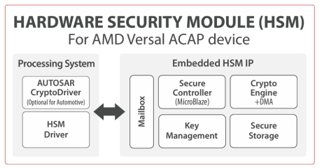
Hardware Security Module (HSM) for AMD Xilinx Versal ACAP device
- The HSM IP module is a Hardware Security Module for a wide range of applications.
- It is developed according to the guidelines set out by the EVITA project and is meant to be implemented on a AMD Xilinx Versal ACAP device.
- It supports TrustZone.
-
GDDR6 PHY IP on GF 12nm LPP
- The UniIC GDDR6 PHY,subsequently referred to as the UNIIC_GD6PHY, is designed for performance and power efficiency, its target is to deliver industry-leading data rates of up to 12Gbps/13Gbps/14Gbps and is compatible with JEDEC standard JEDEC250 and DFI 3.1
- The UNIIC_GD6PHY is used to transfer the Command/Address and Datas between the memory controller and the GDDR6 DRAM device; _x000D_ The UNIIC_GD6PHY is available in Global Foundries FinFET 12LPP technology
- The UNIIC_GD6PHY is fully documented and comes with a comprehensive set of deliverables for ease of system modeling and integration.
-
DDR5 & DDR4 COMBO IO for memory controller PHY, 4800Mbps on TSMC 12nm
- The DDR5&DDR4 COMBO IO is used to transfer the Command/Address/Clk and Data between the memory controller PHY and the DRAM device
- The TX is designed to send information from PHY to DRAM and RX is designed to receive information which is from DRAM._x000D_ It supports DDR5&DDR4 interface
- The DDR5 DQ data rate can be up to 4800Mb/s, and the DDR4 DQ data rate can be up to 3200Mb/s and CA is SDR mode.
-
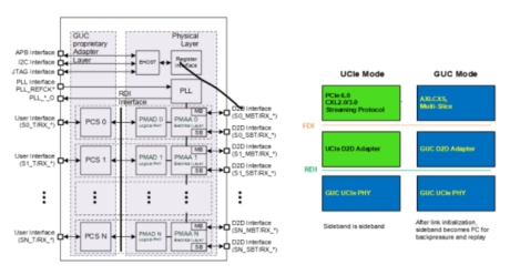
TSMC CLN5FF GUCIe LP Die-to-Die PHY
- IGAD2DY11A is an LP (Low Power) Die-to-Die (D2D) PHY for SoIC-X Face-to-Face advanced package.
- This GUCIe PHY not only supports UCIe specification rev 1.1 compliance physical layer and Raw D2D interface (RDI) but also optionally provides the
-
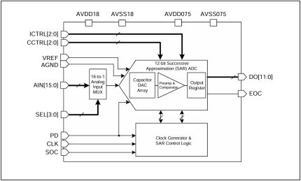
12-bit ADC on Samsung 8nm LN08LPP
- The sf_adc0802x_ln08lpp_306011 is a 1.8V/0.75V dual supply-voltage 16-ch 12-bit analog-to-digital converter (ADC) that supports conversion rate (FS) up to 1MS/s, designed in 8nm CMOS FinFET process.
- It consists of a 16-to-1 analog input MUX, a successive approximation (SAR) type monolithic ADC, a clock generator, and level-shifters for low voltage digital interface.