DDR SDRAM PHY IP
Filter
Compare
153
IP
from
14
vendors
(1
-
10)
-
SDRAM DDR Controller
- Dolphin Technology offers high performance DDR4/3/2 SDRAM and LPDDR5/4x/4/3/2 SDRAM Memory Controller IP across a broad range of process technologies.
-
DDR PHY
- Dolphin's hardened DDR4/3/2 SDRAM PHY and LPDDR5/4x/4/3/2 SDRAM PHY IP is a silicon-proven, Combo PHY supporting speeds up to 4266 Mbps.
- It is fully compliant with the DFI 4.0 specification, and features include slew rate control, per-bit de-skew, gate training, read and write leveling and built-in self test (BIST).
- In addition, our PHY IP is optimized to provide a complete solution when combined with Dolphin's DDRx and LPDDRx SDRAM Memory Controller IP.
-
DDR multi PHY
- Compatible with JEDEC standard DDR2/DDR3/LPDDR (or Mobile DDR)/ /LPDDR2/LPDDR3 SDRAMs
- Operating range of 100MHz (200Mb/s) to 533MHz(1066Mb/s) in DDR2/DDR3/LPDDR2/LPDDR3 modes
- Operating range of DC to 200MHz in Mobile DDR mode
- PHY Utility Block (PUBL) component
-
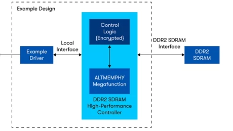
DDR and DDR2 SDRAM Controller with ALTMEMPHY Intel® FPGA IP
- The DDR and DDR2 SDRAM Controller with ALTMEMPHY Intel FPGA Intellectual Property (IP) provides simplified interfaces to industry-standard DDR SDRAM and DDR2 SDRAM
- The DDR and DDR2 SDRAM Controller with ALTMEMPHY Intel FPGA IP core work in conjunction with the ALTMEMPHY physical interface IP function
- The controllers offer a half-rate interface and a full-rate interface to the customer application logic
- For exact device support, please refer to the user guide.
-
LPDDR6/5X/5 PHY V2 - TSMC N6
- The LPDDR6/5X/5 PHY IP enables ASICs, ASSPs, system-on-chips (SoCs), and system-in-package applications requiring high-performance LPDDR6, LPDDR5X, and/or LPDDR5 SDRAM interfaces operating at up to 14.4 Gbps
- With flexible configuration options, the LPDDR6/5X/5 PHY IP can be used in a variety of applications supporting LPDDR6, LPDDR5X, and/or LPDDR5 SDRAMs, precisely targeting the specific power, performance, and area (PPA) requirements of these systems
- LPDDR6 SDRAM’s combination of high bandwidth, capacity, low power, and cost effectiveness makes LPDDR6/5X/5 SDRAMs an attractive solution for traditional and new markets
- The LPDDR6/5X/5 PHY IP is designed to appeal to a variety of applications including: * Traditional mobile environments * Consumer products * Automotive solutions * Artificial intelligence * Data center applications

-
LPDDR6/5X/5 PHY V2 - TSMC N5A for Automotive, ASIL B Random, AEC-Q100 Grade 2
- The LPDDR6/5X/5 PHY IP enables ASICs, ASSPs, system-on-chips (SoCs), and system-in-package applications requiring high-performance LPDDR6, LPDDR5X, and/or LPDDR5 SDRAM interfaces operating at up to 14.4 Gbps
- With flexible configuration options, the LPDDR6/5X/5 PHY IP can be used in a variety of applications supporting LPDDR6, LPDDR5X, and/or LPDDR5 SDRAMs, precisely targeting the specific power, performance, and area (PPA) requirements of these systems
- LPDDR6 SDRAM’s combination of high bandwidth, capacity, low power, and cost effectiveness makes LPDDR6/5X/5 SDRAMs an attractive solution for traditional and new markets
- The LPDDR6/5X/5 PHY IP is designed to appeal to a variety of applications including: * Traditional mobile environments * Consumer products * Automotive solutions * Artificial intelligence * Data center applications

-
LPDDR6/5X/5 PHY V2 - TSMC N5
- The LPDDR6/5X/5 PHY IP enables ASICs, ASSPs, system-on-chips (SoCs), and system-in-package applications requiring high-performance LPDDR6, LPDDR5X, and/or LPDDR5 SDRAM interfaces operating at up to 14.4 Gbps
- With flexible configuration options, the LPDDR6/5X/5 PHY IP can be used in a variety of applications supporting LPDDR6, LPDDR5X, and/or LPDDR5 SDRAMs, precisely targeting the specific power, performance, and area (PPA) requirements of these systems
- LPDDR6 SDRAM’s combination of high bandwidth, capacity, low power, and cost effectiveness makes LPDDR6/5X/5 SDRAMs an attractive solution for traditional and new markets
- The LPDDR6/5X/5 PHY IP is designed to appeal to a variety of applications including: * Traditional mobile environments * Consumer products * Automotive solutions * Artificial intelligence * Data center applications

-
LPDDR6/5X/5 PHY V2 - TSMC N4P
- The LPDDR6/5X/5 PHY IP enables ASICs, ASSPs, system-on-chips (SoCs), and system-in-package applications requiring high-performance LPDDR6, LPDDR5X, and/or LPDDR5 SDRAM interfaces operating at up to 14.4 Gbps
- With flexible configuration options, the LPDDR6/5X/5 PHY IP can be used in a variety of applications supporting LPDDR6, LPDDR5X, and/or LPDDR5 SDRAMs, precisely targeting the specific power, performance, and area (PPA) requirements of these systems
- LPDDR6 SDRAM’s combination of high bandwidth, capacity, low power, and cost effectiveness makes LPDDR6/5X/5 SDRAMs an attractive solution for traditional and new markets
- The LPDDR6/5X/5 PHY IP is designed to appeal to a variety of applications including: * Traditional mobile environments * Consumer products * Automotive solutions * Artificial intelligence * Data center applications

-
LPDDR6/5X/5 PHY V2 - TSMC N4C
- The LPDDR6/5X/5 PHY IP enables ASICs, ASSPs, system-on-chips (SoCs), and system-in-package applications requiring high-performance LPDDR6, LPDDR5X, and/or LPDDR5 SDRAM interfaces operating at up to 14.4 Gbps
- With flexible configuration options, the LPDDR6/5X/5 PHY IP can be used in a variety of applications supporting LPDDR6, LPDDR5X, and/or LPDDR5 SDRAMs, precisely targeting the specific power, performance, and area (PPA) requirements of these systems
- LPDDR6 SDRAM’s combination of high bandwidth, capacity, low power, and cost effectiveness makes LPDDR6/5X/5 SDRAMs an attractive solution for traditional and new markets
- The LPDDR6/5X/5 PHY IP is designed to appeal to a variety of applications including: * Traditional mobile environments * Consumer products * Automotive solutions * Artificial intelligence * Data center applications

-
LPDDR6/5X/5 PHY V2 - TSMC N3P
- The LPDDR6/5X/5 PHY IP enables ASICs, ASSPs, system-on-chips (SoCs), and system-in-package applications requiring high-performance LPDDR6, LPDDR5X, and/or LPDDR5 SDRAM interfaces operating at up to 14.4 Gbps
- With flexible configuration options, the LPDDR6/5X/5 PHY IP can be used in a variety of applications supporting LPDDR6, LPDDR5X, and/or LPDDR5 SDRAMs, precisely targeting the specific power, performance, and area (PPA) requirements of these systems
- LPDDR6 SDRAM’s combination of high bandwidth, capacity, low power, and cost effectiveness makes LPDDR6/5X/5 SDRAMs an attractive solution for traditional and new markets
- The LPDDR6/5X/5 PHY IP is designed to appeal to a variety of applications including: * Traditional mobile environments * Consumer products * Automotive solutions * Artificial intelligence * Data center applications
