DDR DLL PHY IP
Filter
Compare
9
IP
from
8
vendors
(1
-
9)
-
DDR multi PHY
- Compatible with JEDEC standard DDR2/DDR3/LPDDR (or Mobile DDR)/ /LPDDR2/LPDDR3 SDRAMs
- Operating range of 100MHz (200Mb/s) to 533MHz(1066Mb/s) in DDR2/DDR3/LPDDR2/LPDDR3 modes
- Operating range of DC to 200MHz in Mobile DDR mode
- PHY Utility Block (PUBL) component
-
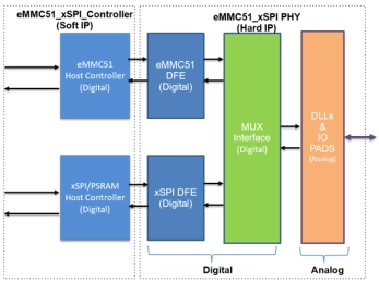
xSPI + eMMC Combo PHY IP
- This IP integrates both xSPI (Expanded Serial Peripheral Interface) and eMMC 5.1 PHY (Physical Layer) into a single unified solution, enabling support for two distinct memory protocols within the same IP.
- By combining the PHY layers for both interfaces, the design simplifies system integration, reduces area and pin count, and enhances design flexibility for SoCs that require both boot and high-speed storage functionality.
-
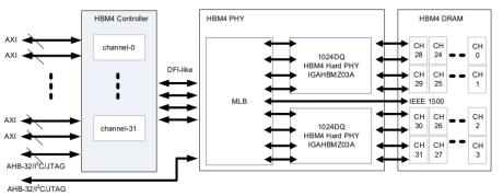
TSMC CLN3FFP HBM4 PHY
- IGAHBMZ03A is a High Bandwidth Memory 4 Physical Layer (HBM4 PHY) that is compliant with JEDEC HBM4 DRAM Specification JESD270-4.
- Fabricated in the TSMC 3 nm Advanced process node (N3P), it supports the data rate up to 12 Gbps per data pin in the DDR PHY Interface (DFI)-like 1:4 clock frequency ratio (HBM4 controller clock: WDQS = 1:4).
-
DDR multiPHY IP
- Support for JEDEC standard DDR2, DDR3/3L/3U, LPDDR, and LPDDR2 SDRAMs
- When combined with a Synopsys Universal DDR digital controller core and Verification IP Synopsys provides a complete multi-protocol DDR interface IP solution
- Scalable architecture that supports from 0 to 1066 Mbps
- DFI 2.1 interface to controller

-
DDR3/ DDR2 Combo PHY IP - 1866Mbps (Silicon Proven in UMC 40LP)
- Supports DDR3/DDR2 SDRAM
- DDR3 JEDEC standard 1.5v I/O (SSTL_15- compatible)
- DDR2 JEDEC standard 1.8v I/O (SSTL_18- compatible)
- 16 bits width, Single Channel DDR3/DDR2 SDRAM Interface.
-
DDR4/ DDR3 Combo PHY IP - 2400Mbps (Silicon Proven in UMC 28HPC+)
- Supports DDR4/DDR3 SDRAM
- DDR4 JEDEC standard 1.2v I/O (POD_12 I/O)
- DDR3 JEDEC standard 1.5v I/O (SSTL_15-compatible)
- 16 bits width, Single Channel DDR4/DDR3 SDRAM Interface.
-
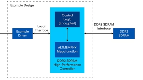
DDR and DDR2 SDRAM Controller with ALTMEMPHY Intel® FPGA IP
- The DDR and DDR2 SDRAM Controller with ALTMEMPHY Intel FPGA Intellectual Property (IP) provides simplified interfaces to industry-standard DDR SDRAM and DDR2 SDRAM
- The DDR and DDR2 SDRAM Controller with ALTMEMPHY Intel FPGA IP core work in conjunction with the ALTMEMPHY physical interface IP function
- The controllers offer a half-rate interface and a full-rate interface to the customer application logic
- For exact device support, please refer to the user guide.
-
DDR2 SDRAM Controller
- Supports industrial standard Double Data Rate (DDR) and Double Date Rate2 (DDR2) SDRAM from 64Mbit to 2Gbit device sizes.
- Page hit detection to support multiple column accesses within the same row.
- Pipeline access enables continuous data bursting and hidden active commands, even in the case of page misses.
- Issue precharge, active and read/write commands to multiple banks at the same time.