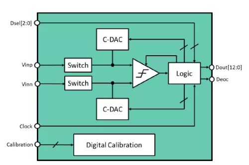
The IP consists of a Successive Approximation Register (SAR) architecture ADC using charge-redistribution technique. The ADC IP is configurable regarding resolution (6-13 bit) and sample rate (up to 10 kS/s) and power consumption down to 1.9 uW. The input voltage range is quasi-ra il -to-ra il guaranteeing more than +-1.7 V@ 1.8 V power supply. An optional calibration technique can be applied to compensate degraded mismatch behavior of technology capacitors.
The ADC IP is applied for industrial and automotive ASIC products.
The ADC IP is silicon evaluated using the XFAB XT018 process. Measurement results and samples are available. The ADC IP was migrated to GF 22FDX and TSMC BCD180 technology with sampling rates up to 2 MS/s.
Fraunhofer IIS/EAS provides a detailed documentation and support for the IP integration. Modifications, extensions and technology ports of the IP are available on request.
Ultra-Low Power 6 - 13 Bit 1-10 kS/s 1.9 uW SAR ADC
Overview
Key Features
- Resolution: 6 - 13 bit
- Conversion rate: up to 10 kS/s
- Power consumption: 1.9 uW @ 0.5 kS/s
- ENOB: 12.6 bit
- Supply voltage: 1.8 V
- Operation clock: 140 kHz
- Differential input: +- 1.7 V
- Silicon area: 0.09 mm2
Benefits
- Low design risk due to silicon evaluated design
- Easy to use input due to integrated input buffer
- Selectable power consumption due to integrated automatic power-down function
- Task dependent selectable resolution
- Flexible use due to single-conversion and continous-conversion mode
Block Diagram
Applications
- Automotive
- Industrial
Deliverables
- GDSII data
- Simulation model
- Documentation
- Silicon validation report
- Integration support
Technical Specifications
Foundry, Node
XFAB XT018
Maturity
silicon evaluated
Availability
now