A Platform for Performance Validation of Memory Controllers
By Ramchandra V, Manikandan Panchapakesan, Haridas V
NXP Semiconductors, Bangalore INDIA
Abstract :
With growing gap between processor and memory speeds, the memory bandwidth has become performance bottleneck for media applications. The memory controller designs are getting optimized to reduce the latencies added by them. It is necessary to prove the performance of memory controller on prototypes. It has been observed that the performance calculated in simulations is very difficult to achieve on prototype board. This is mainly because of subsystem limitations. The present paper illustrates how a generic prototype can be designed and used to prove the memory controller performance. HW based performance monitor unit is designed and used in simulation and prototype validation. The proposed methodology has been used in performance validation of External memory controller for Cellular Ram and NOR flash.
1. Introduction
With the development of processing technology, more and more complex functionality can be incorporated into today’s System On Chip designs. At the same time market forces have led to greater time-to-market pressure. IP based SoC design methodology improves design productivity by increasing the design abstract level by moving from RTL to system level and thereby provide improved reusability and configurability. However it has been observed that as the IP is made more and more reusable and configurable, the performance of IP is getting affected at the cost of extra features. The media applications like third generation chipsets are designed to support higher data rates. The usage of high performance microprocessor with memory management unit (e.g., ARM926J-S) is increasing. The Integrated hardware encoders and decoders (instead of software codec) are being used to support high performance. In order to give good and high quality product the bandwidth requirement of the product has to be met by the SoC design.
The semiconductor industry has now started looking at each and every aspect of SoC design to tune it to the highest possible bandwidth. One of the aspect where most of the designs concentrate is the system and data memory. There are many kinds of memories which are used in SoC designs including SRAMs, NOR Flash, NAND Flash, DDR etc. These memories are accessed with the dedicated memory controller. For a high performance design the path from processor to memory should have very minimal latency.
The paper is organized in the following manner. First a short discussion on the performance metrics is given (sec ‘2’), followed with the performance calculation setup in simulation (sec ‘3’). This is followed with a performance calculation setup on FPGA prototype (sec ‘4’) which includes issues faced, performance monitor unit design and usage. Finally the results in section ‘5’ is followed by conclusions in section ‘6’.
2. Performance metrics
The quality of the performance results is ultimately determined by the environment in which the data is collected. It is also important to know that what are the different performance metrics used to represent the performance. Below are the metrics which are used in this paper.
Bandwidth is the capacity for a given system to transfer data over a bus. It is measured as a bit rate expressed in bits/s or multiples of it (kb/s Mb/s etc.). Latency is the delay between the initiation of a transfer by a sender and the receipt of that transfer by a receiver. The efficiency determines the percentage of clock cycles where data is actually transferred. The efficiency relates the achieved bandwidth to the maximum peak bandwidth. Throughput is the amount of useful data transfer which only includes the actual data transfer and not the address of memory locations. It is possible that the system may not be able to use the memory bus every cycle because of the processors internal calculation cycles. The Bus Utilization refers to the percentage of data cycles and wait or busy cycles.
3. Performance Calculation setup in simulation
The memory controller IP has specman based verification testbench. The same has been extended for doing the performance calculation. The block diagram of the testbench is depicted in figure 1.
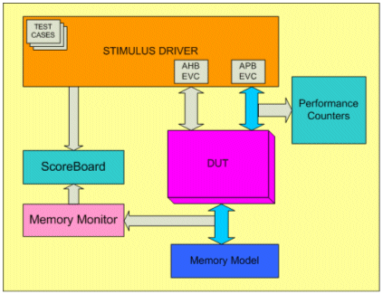
Figure 1. Performance calculation in Simulation
The APB eVC will generate the APB transfers to set the configuration via control/ status registers of the memory controller. The stimulus driver will generate stimuli, which are translated into APB transfers. The APB monitor checks that the APB protocol is not violated. The APB monitor is able to share information about the traffic with the monitor of the stimulus driver. The AHB-Lite eVC will generate stimuli on the data port. The generated stimuli are bound to certain constraints, like command delays and burst size. The AHB-Lite monitor performs protocol checks and is able to share information about the traffic with the stimulus driver’s monitor. The data scoreboard will check the data consistency between the data bus of the memory controller and the memory transactions.
The performance test case are written for following cases
Data Cycle = HSEL = '1' & HREADY= '1' & (HTRANS = "10" or HTRANS = "11")
Busy Cycle = (HSEL= '1' & HREADY = '0')
4. Performance Calculation setup on prototype
Architectural considerations for prototype
The purpose of the exercise is to create the platform which should be able to do continuous streaming of data for read and write operations. The platform should have minimum possible latency between processor and memory controller. Use of DMA controller which can do streaming by reading from one memory and writing to memory controller under test is also one of the options that can be used to generate the streaming data. However the scenarios expected by validation test’s may not be generated. Like INCR4 or INCR8 may not be continuously generated if the DMA controller does not have programmability for these bursts. Ideally there should not be any protocol conversion bridges/adaptors on this path. This is because as per ARM guidelines if the write burst transfer (INCR4, INCR8) is non bufferable (AHB), then it can be split into single transfers. If bridges can not be avoided then the bufferable transfer has to be created from the software. The architecture should provide some mechanism (either in SW or in HW) to calculate the time taken for the transfers to complete.
Software considerations
In case of ‘e’ based simulation the AHB evc was able to do data streaming with out any delay between the transfers. However in Hardware prototype we can no longer use the same ‘e’ case as the processor (say ARM) has to do this task. We have to use high level languages like ‘C’ which the cross compiler will convert to processor assembly code. It has been observed that using ‘C’ language for streaming tests is not that efficient as we want. Also the ARM code generated from cross compiler may not give the exact scenarios like INCR4 or INCR8 streaming in full test. In order to achieve the exact streaming of INCR4 kind of bursts, the assembly level routines will be generally used. These routines should also be capable of writing/reading such transfers continuously without any gap. The read routine should be able to do on-the-fly sanity check for written data. Typical example would be using “ldmia r0!, { r1 - r8 }” for INCR8 reading and “stmia r0!, { r1 - r8 }”. In order to create the streaming test we had to use the mix of ‘C’ code and assembly code.
Prototype setup
The architectural block diagram of the setup for memory controller prototype is shown in figure 2. Here we have a CPU subsystem consisting of the ARM 926EJ-S processor along with I/D Cache and TCM, Boot and application Memory, DMAC, INTC and Design under test.
Specially designed Performance Monitor Unit is also added. The purpose of this block is to keep track of Data cycles, slave busy cycles, master busy cycles etc. for the programmed start address and end address. The detailed design of this Unit will be discussed in next section.
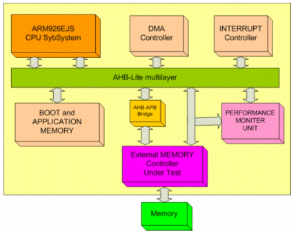
Figure 2. Validation setup
Performance monitor unit
The block diagram of performance monitor unit is shown figure 3. AHB state machine probes the present state of the AHB bus. There are several registers implemented which hold the value of start address, end address, data cycles, busy cycles. These registers are written and read from APB slave port. The purpose of Start address register is that it
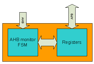
Figure 3. Performance monitor
holds the starting address of first transfer in the test case. This address corresponds to memory location which will be accessed using data port of memory controller. Similarly the end address is the last address of the last transfer in the test case.
As an example for AHB bus the Data Cycles counter will be incremented for following condition
Data Cycle = HSEL = '1' & HREADY= '1' & (HTRANS = "10" or HTRANS = "11")
Slave busy cycle = (HSEL= '1' & HREADY = '0')
Master BusyIdle cycle = (HSEL= '0' & HREADY = '1') or (HREADY= '1' & HSEL= '1' & (HTRANS = “01” or HTRANS = “00”))
So totalcycles = DataCycles + SlavebusyCycles + MasterBusyIdleCycles.
5. Tests and results
The performance tests similar to that one in ‘e’ based simulation setup are rewritten in a mixture of ‘C’ and ARM assembly code. However in case of ‘e’ the data sanity check was done in parallel to streaming & receiving the data, but in case of prototype we have to do this differently. If we do the data sanity checks parallel to data transfer, we will no longer be able to do streaming with out gap between consecutive transfers. So what we did is we did the data sanity checks at the end of the test case.
The representative algorithm for INCR4 burst write performance test is given below.
Reset the Start address & end address , counter registers in the performance monitor
Call assembly routine which has 100 INCR4 writes.
Read the data cycles, busy cycles counters from
performance monitor for the AHB bus
Read the data cycles, busy cycles counters from performance monitor for the memory bus.
Calculate the efficiency, the bandwidth and the latency
The formulas used are
The Bus utilization will be reported as percentage of each kind of cycles
(In the similar way read algorithm is written)

Figure 4. Write transaction observed with logic analyzer at memory interface
PERFORMACE
6. Conclusion
Here we presented the differences in the memory performance validation in simulation and prototype. The way of doing performance calculations in simulation and prototype validation is different. It is very easy to create tests and calculate the performance in simulation. However in order to get similar tests and results on prototype is tricky.
References
[1] E Language reference manual
[2] The Design Warrior's Guide to FPGAs - Clive Max Maxfield
[3] ARM training material
[4] AMBA specification 2.0
[5] www.wikipedia.org
NXP Semiconductors, Bangalore INDIA
Abstract :
With growing gap between processor and memory speeds, the memory bandwidth has become performance bottleneck for media applications. The memory controller designs are getting optimized to reduce the latencies added by them. It is necessary to prove the performance of memory controller on prototypes. It has been observed that the performance calculated in simulations is very difficult to achieve on prototype board. This is mainly because of subsystem limitations. The present paper illustrates how a generic prototype can be designed and used to prove the memory controller performance. HW based performance monitor unit is designed and used in simulation and prototype validation. The proposed methodology has been used in performance validation of External memory controller for Cellular Ram and NOR flash.
1. Introduction
With the development of processing technology, more and more complex functionality can be incorporated into today’s System On Chip designs. At the same time market forces have led to greater time-to-market pressure. IP based SoC design methodology improves design productivity by increasing the design abstract level by moving from RTL to system level and thereby provide improved reusability and configurability. However it has been observed that as the IP is made more and more reusable and configurable, the performance of IP is getting affected at the cost of extra features. The media applications like third generation chipsets are designed to support higher data rates. The usage of high performance microprocessor with memory management unit (e.g., ARM926J-S) is increasing. The Integrated hardware encoders and decoders (instead of software codec) are being used to support high performance. In order to give good and high quality product the bandwidth requirement of the product has to be met by the SoC design.
The semiconductor industry has now started looking at each and every aspect of SoC design to tune it to the highest possible bandwidth. One of the aspect where most of the designs concentrate is the system and data memory. There are many kinds of memories which are used in SoC designs including SRAMs, NOR Flash, NAND Flash, DDR etc. These memories are accessed with the dedicated memory controller. For a high performance design the path from processor to memory should have very minimal latency.
The paper is organized in the following manner. First a short discussion on the performance metrics is given (sec ‘2’), followed with the performance calculation setup in simulation (sec ‘3’). This is followed with a performance calculation setup on FPGA prototype (sec ‘4’) which includes issues faced, performance monitor unit design and usage. Finally the results in section ‘5’ is followed by conclusions in section ‘6’.
2. Performance metrics
The quality of the performance results is ultimately determined by the environment in which the data is collected. It is also important to know that what are the different performance metrics used to represent the performance. Below are the metrics which are used in this paper.
Bandwidth is the capacity for a given system to transfer data over a bus. It is measured as a bit rate expressed in bits/s or multiples of it (kb/s Mb/s etc.). Latency is the delay between the initiation of a transfer by a sender and the receipt of that transfer by a receiver. The efficiency determines the percentage of clock cycles where data is actually transferred. The efficiency relates the achieved bandwidth to the maximum peak bandwidth. Throughput is the amount of useful data transfer which only includes the actual data transfer and not the address of memory locations. It is possible that the system may not be able to use the memory bus every cycle because of the processors internal calculation cycles. The Bus Utilization refers to the percentage of data cycles and wait or busy cycles.
3. Performance Calculation setup in simulation
The memory controller IP has specman based verification testbench. The same has been extended for doing the performance calculation. The block diagram of the testbench is depicted in figure 1.

Figure 1. Performance calculation in Simulation
The APB eVC will generate the APB transfers to set the configuration via control/ status registers of the memory controller. The stimulus driver will generate stimuli, which are translated into APB transfers. The APB monitor checks that the APB protocol is not violated. The APB monitor is able to share information about the traffic with the monitor of the stimulus driver. The AHB-Lite eVC will generate stimuli on the data port. The generated stimuli are bound to certain constraints, like command delays and burst size. The AHB-Lite monitor performs protocol checks and is able to share information about the traffic with the stimulus driver’s monitor. The data scoreboard will check the data consistency between the data bus of the memory controller and the memory transactions.
The performance test case are written for following cases
- Write traffic –The traffic generators do continuous write to memory controller data port with AHB single writes, AHB INCR4 Writes, AHB INCR8 Writes.
- Read traffic – The traffic is focused on continuous read from memory controller data port for AHB single read, AHB INCR4 read, AHB INCR8 read.
- Bus Utilization – Here we will do 100 cycles transfer and check if memory controller is doing data transfer or is in wait state for each of AHB single write, AHB INCR4 write, AHB INCR8 Write.
Data Cycle = HSEL = '1' & HREADY= '1' & (HTRANS = "10" or HTRANS = "11")
Busy Cycle = (HSEL= '1' & HREADY = '0')
4. Performance Calculation setup on prototype
Architectural considerations for prototype
The purpose of the exercise is to create the platform which should be able to do continuous streaming of data for read and write operations. The platform should have minimum possible latency between processor and memory controller. Use of DMA controller which can do streaming by reading from one memory and writing to memory controller under test is also one of the options that can be used to generate the streaming data. However the scenarios expected by validation test’s may not be generated. Like INCR4 or INCR8 may not be continuously generated if the DMA controller does not have programmability for these bursts. Ideally there should not be any protocol conversion bridges/adaptors on this path. This is because as per ARM guidelines if the write burst transfer (INCR4, INCR8) is non bufferable (AHB), then it can be split into single transfers. If bridges can not be avoided then the bufferable transfer has to be created from the software. The architecture should provide some mechanism (either in SW or in HW) to calculate the time taken for the transfers to complete.
Software considerations
In case of ‘e’ based simulation the AHB evc was able to do data streaming with out any delay between the transfers. However in Hardware prototype we can no longer use the same ‘e’ case as the processor (say ARM) has to do this task. We have to use high level languages like ‘C’ which the cross compiler will convert to processor assembly code. It has been observed that using ‘C’ language for streaming tests is not that efficient as we want. Also the ARM code generated from cross compiler may not give the exact scenarios like INCR4 or INCR8 streaming in full test. In order to achieve the exact streaming of INCR4 kind of bursts, the assembly level routines will be generally used. These routines should also be capable of writing/reading such transfers continuously without any gap. The read routine should be able to do on-the-fly sanity check for written data. Typical example would be using “ldmia r0!, { r1 - r8 }” for INCR8 reading and “stmia r0!, { r1 - r8 }”. In order to create the streaming test we had to use the mix of ‘C’ code and assembly code.
Prototype setup
The architectural block diagram of the setup for memory controller prototype is shown in figure 2. Here we have a CPU subsystem consisting of the ARM 926EJ-S processor along with I/D Cache and TCM, Boot and application Memory, DMAC, INTC and Design under test.
Specially designed Performance Monitor Unit is also added. The purpose of this block is to keep track of Data cycles, slave busy cycles, master busy cycles etc. for the programmed start address and end address. The detailed design of this Unit will be discussed in next section.

Figure 2. Validation setup
Performance monitor unit
The block diagram of performance monitor unit is shown figure 3. AHB state machine probes the present state of the AHB bus. There are several registers implemented which hold the value of start address, end address, data cycles, busy cycles. These registers are written and read from APB slave port. The purpose of Start address register is that it

Figure 3. Performance monitor
holds the starting address of first transfer in the test case. This address corresponds to memory location which will be accessed using data port of memory controller. Similarly the end address is the last address of the last transfer in the test case.
As an example for AHB bus the Data Cycles counter will be incremented for following condition
Data Cycle = HSEL = '1' & HREADY= '1' & (HTRANS = "10" or HTRANS = "11")
Slave busy cycle = (HSEL= '1' & HREADY = '0')
Master BusyIdle cycle = (HSEL= '0' & HREADY = '1') or (HREADY= '1' & HSEL= '1' & (HTRANS = “01” or HTRANS = “00”))
So totalcycles = DataCycles + SlavebusyCycles + MasterBusyIdleCycles.
5. Tests and results
The performance tests similar to that one in ‘e’ based simulation setup are rewritten in a mixture of ‘C’ and ARM assembly code. However in case of ‘e’ the data sanity check was done in parallel to streaming & receiving the data, but in case of prototype we have to do this differently. If we do the data sanity checks parallel to data transfer, we will no longer be able to do streaming with out gap between consecutive transfers. So what we did is we did the data sanity checks at the end of the test case.
The representative algorithm for INCR4 burst write performance test is given below.
Reset the Start address & end address , counter registers in the performance monitor
Call assembly routine which has 100 INCR4 writes.
Read the data cycles, busy cycles counters from
performance monitor for the AHB bus
Read the data cycles, busy cycles counters from performance monitor for the memory bus.
Calculate the efficiency, the bandwidth and the latency
The formulas used are
Efficiency = (No_of_Bytes_transferred / totalcycles) *100
Throughput = (No_of_Bytes_transferred / totalcycles) * Frequency
Throughput = (No_of_Bytes_transferred / totalcycles) * Frequency
The Bus utilization will be reported as percentage of each kind of cycles
(In the similar way read algorithm is written)

Figure 4. Write transaction observed with logic analyzer at memory interface
PERFORMACE
| Type | Bytes | Cycles | Efficiency % | Throughput at 78 MHz |
| SINGLE | 400 | 695 | 57.55 | 44.89 |
| INCR4 | 1600 | 1295 | 123.55 | 96.37 |
| INCR8 | 3200 | 2095 | 152.74 | 119.14 |
| Total | | | | 86.8 MB |
6. Conclusion
Here we presented the differences in the memory performance validation in simulation and prototype. The way of doing performance calculations in simulation and prototype validation is different. It is very easy to create tests and calculate the performance in simulation. However in order to get similar tests and results on prototype is tricky.
References
[1] E Language reference manual
[2] The Design Warrior's Guide to FPGAs - Clive Max Maxfield
[3] ARM training material
[4] AMBA specification 2.0
[5] www.wikipedia.org
Related Semiconductor IP
- Memory Controller
- Fault Tolerant DDR2/DDR3/DDR4 Memory controller
- HYPERBUS™ Memory Controller
- xSPI Multiple Bus Memory Controller
- HBM Memory Controller
Related Articles
- DDR3 memory interface controller IP speeds data processing applications
- Behavioral Model of a DDR Memory Controller in a DFi - Frequency Ratio System
- Metric Driven Verification of Reconfigurable Memory Controller IPs Using UVM Methodology for Improved Verification Effectiveness and Reusability
- Smart way to memory controller verification: Synopsys Memory VIP
Latest Articles
- SNAP-V: A RISC-V SoC with Configurable Neuromorphic Acceleration for Small-Scale Spiking Neural Networks
- An FPGA Implementation of Displacement Vector Search for Intra Pattern Copy in JPEG XS
- A Persistent-State Dataflow Accelerator for Memory-Bound Linear Attention Decode on FPGA
- VMXDOTP: A RISC-V Vector ISA Extension for Efficient Microscaling (MX) Format Acceleration
- PDF: PUF-based DNN Fingerprinting for Knowledge Distillation Traceability