An efficient approach to evaluate Dynamic and Static voltage-drop on a multi-million transistor SoC design
Set-Top-Box SoC wire-bond and its adaptation for a flipchip : testcase and results
By Abhishek Nigam, Vivek Sinha (ST Microelectronics)
Abstract
As Set-Top-Box(STB) SoC designs become extremely complex with multi-million gates, lowering of voltage supplies, and multiple clock domains including high and low frequencies, evaluating the power-integrity of a chip has become one of the key challenges in design and ensuring good yield.
This paper describes the methodology and technology we used, to assess full-chip dynamic and static IR-drop for such complex and huge SoCs. Firstly, it outlines power-grid weakness and hot spot exploration using a testcase of STB SoC in 65nm WireBond and Flipchip variants. Additionally, it outlines the complexity in performing voltage drop analysis in vector-less mode without a VCD in terms of methodology and technology, specifically due to flipchip complexity.
Finally, the paper describes the key implementation approaches using Ansys’ RedHawk tool and power-trends observed on such SoCs. Using this approach SoC designers will be in a position to analyze dynamic voltage waveforms for every place-able instance on a power-grid, early in the design process, explore “hot spots”, as well as verify full-chip power-integrity in the design flow - a value-ad to SoC implementation flows.
Introduction
1. Set-Top-Box SoC designs are complex, typically with over 100 million transistors, having multiple frequencies and low voltage supply of 1.1V in 65 nm technology node. In the past, others have tried to evaluate P/G weakness, computed the resistance of each cell from its P/G pins to the power pads, and then generated a report identifying high resistance paths, static voltage drop analysis and hot-spot exploration on SoC with Wirebond package. Most of the times undetected Silicon IR drop may lead to appropriate voltage not reaching a transistor, which can to an extent be compensated by increasing the supply at board level. In extreme cases, it could also lead to customer-returns, because of a Timing Analysis failure, whose root-cause could be eventually found to be due to higher-than-rated, voltage drop on operation. Dynamic Voltage drop is something that cannot be modeled by pure traditional Static Timing Analysis. So, the need to calculate and model the dynamic IR drop on SoCs was a driver for formulation and execution of the idea as explained in this paper. A specific problem was the non-feasibility of creating a Value Change Dump (VCD) file for “functional mode” for such an extremely large SoC which may contain actual switching information. Ansys Redhawk tool provided a dynamic simulator which uses an internal statistical approach towards vector-less dynamic IR drop analysis but which covers realistic worst case switching scenarii. This methodology was exploited on STB variants (wire-bond and flipchips), as summarized in Figure 11, to assess their Dynamic IR drop and compare with corresponding Static results. This approach can be re-used on similar large SoCs to evaluate their Dynamic voltage drop behaviours, and better prepared before Si-out.
2. Scope of STB SOC WireBond(WB) and FlipChip(FC) analysis:
While calculating dynamic voltage drop on STB Flip chip variants, the added complexity was that they were created keeping location of IO-pads at the die-edge which is the classical position as in Wirebond pad-limited SoCs. It means, power supply eventually arrives to the core, from the die-edge. This methodology was done specific to both STB Flip chip PG tapes, as we were constrained by mask-layer compatibility to previous wire bond chip. We had to ensure base-layer compatibility up to Metal-6, which is why we were obliged to preserve the classical IO pads at the periphery, even though there existed central power bumps. In other words, the routing from central power bumps up to the pad-openings is also contributing to IR drop, in this case.
1. The STB design statics and power summary representation in Figure 1:
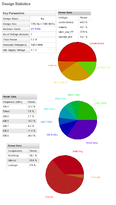
Figure 1.
Power summary in Figure 1 is Cell Type based, Frequency based and power components based. Switching scenario is derived statically and depends on several design-aware factors such as:
- Area with structural weakness: Uneven Pad placement, weakly connected mesh and High resistive paths.
- Instance Timing Windows.
- Logic/power/toggle rate of instances.
We have supplied known core power data of 1.2Watts, Redhawk performs scaling of the toggle rate for the block, instance or cell to achieve more accurate analysis for instances. Dominant operating frequency on the chip is defined as 100MHz, the lowest frequency that includes 96% of the power consumption on the chip. STA file from Primetime was generated in Functional mode Worst
case corner. SPEF files are generated through Synopsys RC extractor.
2. Design Weakness in STB Wire-bond and Flip-chip variants
Design Weakness is similar as only RDL/package has changed and not Place and Route database.
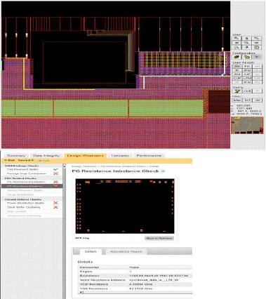
Figure 2
In Static voltage drop, Instance will draw the current all the time, it does not matter when the instance switches. In Dynamic voltage drop, Instances will draw transient current only when it switches. Non-switching instance will draw only leakage current. Dynamic analysis will see the real peak demand current on the chip.
3. Static Voltage drop in STB Wire-bond and Flip-chip variants.
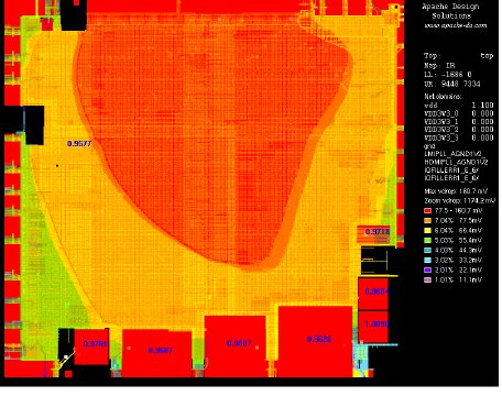
Figure 3
4. Voltage drop analysis in STB WireBond
4.1 Dynamic Voltage drop map and Hot Spot exploration.
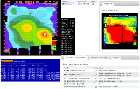
Figure 4
5. Voltage drop analysis in Set-Top-Box SOC FC_2RDL (RDL1 – Alucap , RDL2-Cu)
Certain data, such as redistribution layer (RDL) in Figure 4 and flip-chip bump layer descriptions, are available in GDSII format. This type of data must be converted to DEF/LEF format for integration into Redhawk database. gds2def utility was key, can output smooth 45-degree geometries in DEF for power/ground routing, including IO rings and RDL. Flowchart in Figure 5 depicts adaptability and flexibility in ignoring AP layer only in available top and partition DEF’s design constraint of redhawk for Set-Top-Box SOC Flip-chip in which AP layer was used as first RDL.
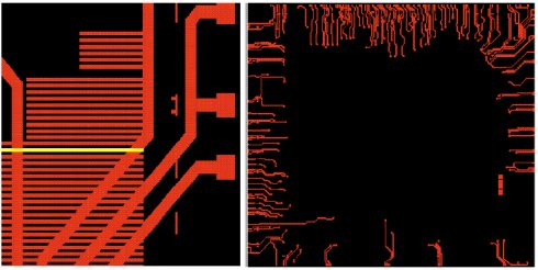
Figure 5
Redistribution Layer in Alucap(AP) can be seen for which need to be extracted for Core Voltage drop.
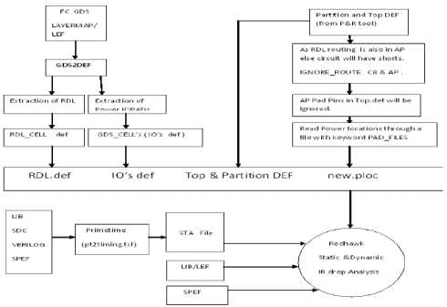
Figure 6 ( Redhawk flow )
5.1 Dynamic Voltage drop map and Hot Spot exploration.
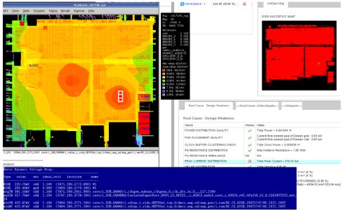
Figure 7
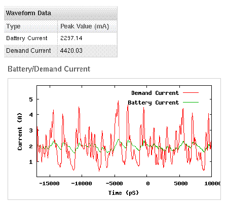
Figure 8
Note : In Figure 3 big difference in demand current and battery current indicates the effectiveness of decaps.Dynamic simulation time, 10000 psec, to include 96.8977% of power consumption on the chip.
6. Voltage drop analysis in Set-Top-Box SOC FC_8ML (RDL1-M8,RDL2-AP)
In this methodology the two redistribution layers used were M8 and AP. M8 layer was used instead of the “external Cu” as compared to the previously described flipchip variant. The Redhawk flow remains the same as shown in Figure 5.
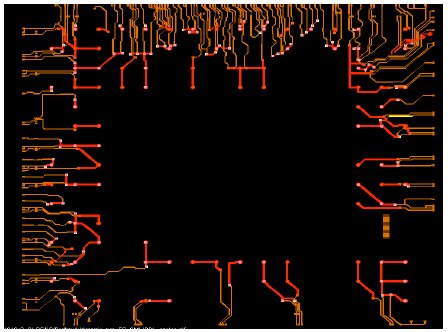
Figure 9
5.2 Dynamic Voltage drop map and Hot Spot exploration.
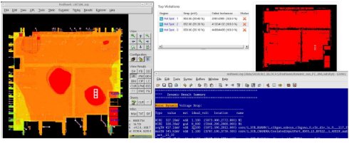
Figure 10
7. Conclusion:
Flow and methodology used by Redhawk tool helped in evaluating Dynamic Voltage drop without a dependency on a VCD for Set-Top-Box SOC , wirebond and flipchip variants. This added value over traditional Static IR drop methods and their limitations. Also, this exercise provided a perspective to the Digtial Convergence Group (DCG) validation team, to understand one of the reasons for the real need to increase supply voltage on Set-Top-Box SOC FC_2RDL Silicon.
SoC Power-trends (Figure 11) of Static versus Dynamic Voltage drop on Wirebond and Flip-chip packages, was demonstrated on representative test-cases. Finally, this approach led to development of a specific CAD method, which has potential for re-use. Limitations are, not having used parasitics netlist for L(di/dt) drop modeling of package and die inductances, and the absence of Apache Power Library(APL) for this 65nm technology node.
Power-figures as observed on Set-Top-Box SOC WB, FC_2RDL and FC_8ML
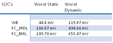
Figure 11
8. Acknowledgements
- Nilabh Srivastava and Gireesh, for their excellent Tool support on Ansys Redhawk usage.
- Neetu Jain , ST Microelectronics
- Arvind Kumar, ST Microelectronics
- Gaurav Sharma, ST Microelectronics
- Vivek Seth, ST Microelectronics
- Naveen Sharma , ST Microelectronics
- Bhanu Prakash , ST Microelectronics
- Rajeev Srivastava , ST Microelectronics
9.1 Appendix -1 : Die-photo.
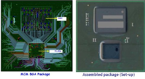
Note: Set-Top-Box SOC FC_2RDL SoC and DDR memory fabricated on the same package!
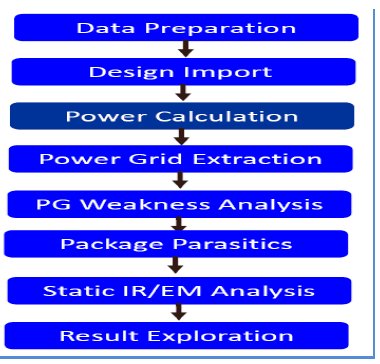
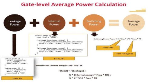
9.2 Appendix -2 Redhawk Tool flow and Gate-level Power Calculation method
Related Semiconductor IP
- NPU IP Core for Mobile
- NPU IP Core for Edge
- Specialized Video Processing NPU IP
- HYPERBUS™ Memory Controller
- AV1 Video Encoder IP
Related White Papers
- Implementing Power Management IP for Dynamic and Static Power Reduction in Configurable Microprocessors using the Galaxy Design Platform at 130nm
- Static and dynamic modeling for high-density memories
- A need for static and dynamic Low Power Verification
- Cache Evaluation Software: A Dynamically Configurable Cache Simulator
Latest White Papers
- Breaking the Memory Bandwidth Boundary. GDDR7 IP Design Challenges & Solutions
- Automating NoC Design to Tackle Rising SoC Complexity
- Memory Prefetching Evaluation of Scientific Applications on a Modern HPC Arm-Based Processor
- Nine Compelling Reasons Why Menta eFPGA Is Essential for Achieving True Crypto Agility in Your ASIC or SoC
- CSR Management: Life Beyond Spreadsheets