DDR IP Hardening - Overview & Advance Tips
By Maulik Patel, Darshan Bhuva and Pooja Bhadaniy from eInfochips (an Arrow Company)
What is DDR?
As the name says Double Data Rate, DDR is the class of memory which transfers data on both the rising and falling edge of clock signal to double data rate without increase in frequency of clock. It uses PLLs (Phase Locked Loops) & self-calibration to reach required timing accuracy.
DDR is most critical IP to SoC’s successful operation, because processors in SoC typically spends the majority of its cycles on reading and writing to DDR memory. The self-calibrating logic precisely measures both the latency and phase difference between DDR clock and system clock and aligns the capture of DDR data within the timing window. Timing calibrating logic also maintains performance of DDR memory as temperature and supply voltage fluctuates during system operation.
DDR Implementation Complexities:
Deep submicron SoC designs integrate DDR memory subsystems that operate at multi-GHz clock rates, resulting in read-write timing margins measured in picoseconds. This concerns Designers about static variations due to process and dynamic variations due to system operating conditions such as temperature and voltage.
-
DDR I/O Timing Requirements are stricter, because data is transferred at both edges of the clock, so the effective data duration is only half a cycle. Logic in DDR generally involves both positive edge triggered flops and negative edge triggered flops and even latches.
-
With the increase in data rates, complexities associated with the timing and signal integrity of the memory interface has become increasingly difficult.
-
For DDR signalling, with the increased frequency, total bit time is reduced, which is evenly divided into setup and hold budget.
DDR IP Hardening:
A DDR Memory Interface IP Solution consists of DDR Controller, PHY & Interface. When we refer to the DDR memory subsystem, we are referring to the host System-on-Chip (SoC) controlling and accessing the DDR memory, the interface and interconnect between the host and DDR memory devices, which is typically a PCB, and the DDR SDRAM device itself.

Some key parameters like DDR modes, frequency ratio and memory data width, must be consistent between DDR PHY and DDR Controller.
DDR PHY Blocks overview
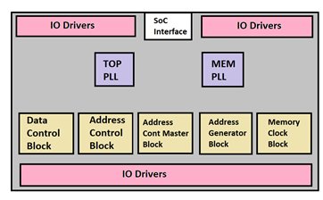
DDR PHY Implementation is divided in internal blocks implementation and TOP implementation. Generally, DDR PHY has five types of blocks as below. Depending on the DDR configuration these block can be changed as per logic.
- Data Control Block: It controls DATA READ/WRITE Operations. It interfaces DQ, associated DM and DQS signal connections to the RAM. Depending on required data width of RAM interface, data blocks are duplicated.
- Address Control Block: It generates RAM control signals, Based on the number of Chip Selects (CS), Address Selections (AS), and other Control Signals.
- Memory clock block: It Provides the DDR clock to the RAMs.
- Address Control Master Block: It controls all Address Control blocks.
- Adders Generator Blocks: It generates DRAM addresses. It provides address signals.
- PLL: DDR also consist of 2 PLL in TOP block. One PLL generates PHY clock whereas other PLL with Memory clock block generates DRAM clock.

For DDR we have Timing Relation between DQ - DQS and CA – clock signals. For DQ-DQS Relation Read/Write Data Macro blocks are responsible. Whereas control address-clock (CA-clk) Relation is responsible for control-address-command interface connection.
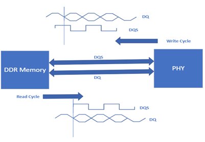
Phase of DQS relative to signal DQ depends on whether it is read or write operation. In Read operation phase, DQS is shifted by 90 degrees with respect to DQ and it will be edge aligned. While in Write operation DQS is central aligned with DQ. As shown in below figure.

Floorplanning Guidelines:
Base of closing DDR is mainly dependent upon Floorplanning. Hence, there are guidelines, which need to be followed during floorplan.
- IO Driver’s placement order should match Data and Address block’s pin order. This way we can reduce criss cross and align signals for better routing. This will help to maintain skew target.
- Signal from Block to IOs should be buffered using script by using same buffer models, higher metal layer, NDR.
- Clock pins are placed at centre to balance skew at both the sides of TOP. Critical signals coming from data and address blocks need special precaution while placing.
- Bump placement needs special attention to reduce Resistance and meet PERC & ESD requirements.
- As the DDR timing constraints are very complex, max delay, and skew related constraints cannot include in SDC. Phase detection logic, PLL logic, Clock Mux needs to be place during floorplan because tool will not do accurate placement. Missing this guidelines causes severe failure in skew.
- Depending on data exchange rate, DDR-protocol, package type, P/G ratios, package decoupling capacitance & PCB decoupling capacitance, Decap requirements are decided. Pre-placement for IO Driver’s decap needed.
Placement Guidelines:
- Core logic Ports connecting SoC need to place very close to port using magnet placement. This way we can reduce data latency.
- Data & Clock Skew Signals, Clock Mux, and Phase detection logic, IO Driver to Core signals should be untouched during the optimization and should be taken care manually.
Top Clocks & Skew Balancing Guidelines:
The following are the clock balancing requirements:
- Phase difference between system clock received by DDR memory and the clock of DDR PHY should be Minimum.
- Setup and Hold time for data bits, control signals and address signals are meeting.
- Duty cycle should be maintained for all the Clock. We do duty cycle distortion checks for the same.
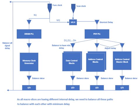
- From functional clock port to input and output flops inside blocks should be balanced with each other
- We try to hardened sub blocks with minimum insertion delay to their flops.
- Post hardening block, while building CTS at top level, we need to consider clock network latency inside the sub-blocks and try to balance each of the flops with more or less same skew value.
- From the Functional and Scan clock port, we build common clock to first level clock fanout pins, and then we build clock tree from clock logic output to all blocks.
- To avoid any extra clock latency, we place PHY clock PLL in centre area of TOP level and Memory clock PLL near to the Memory clock Generator block. Also, the related clock logic to each PLL is placed nearby.
- As we were having high data rate requirement, we used high driver inverters which has symmetrical rise and fall delay and built clock tree manually with higher metal layer, applied NDR and used shielding wherever required to avoid cross talk.
- For the skew requirements of signal nets from the sub blocks to IOs,
- Route with almost same length and resistance to have equal delay.
- Macro cells to IO distance should be minimum
- Use NDR, shielding, higher metal layers for routing
- Add equal numbers of buffers on these nets

MODELLING OF SKEW RELATED STD. CELLs:
In IP there are many hierarchical cells for which the net length should be minimum for those hierarchical cells it is beneficial to make some macro structure which include these cells with the power and signal routing and use it as a macro in the design to minimize the net length. So we can use the extract model from netlist for the same.
Why we model the cells?
- To solve the identical issues of Placement and Routing.
- To ensure constant behaviour for master and slave hierarchical cells.
- To achieve delay element identity.
Library Cell Delay Variation Impacting Skew:
Balancing Skew/Data paths across multiple corners is tough task as delay variation in cells plays vital role in lower technology node. Meeting same skew value for multiple data bit line which are greater than 2000um long, makes this job even harder. Few cases we will understand which are substantially important before fixing timing issues.
1. VT variations across ss/ff
We have seen that across multiple VT, delay variation ratio between ss/ff changes drastically.
Here is example of bufx2:
| VT | Slow Corner-SS | Fast Corner-FF | % Variation |
| ULVT | 18ps | 10ps | 1.8 |
| LVT | 20ps | 9ps | 2.2 |
| SVT | 24ps | 8ps | 3 |
| HVT | 28ps | 7ps | 4 |
2. Setup-Hold Critical Paths and Delay Buffers
DDR have very complex clock constraint. There are many cases where registers are getting multiple clock in functional mode. Frequency for these Clocks are phase shifted. This causes multiple paths to fail for setup and hold. Such cases can be addressed by balancing clock at Mux point. Next step would be lowering down data paths delay by upsize/Vt swap such that it impacts min delay values for these stages as less as possible. Hold may be still violating but Setup may get fixed by minimal margin. To Address Hold using Delay-Buffer may not be wise decision as delay variation is more between SS & FF.
Here is example of delay-bufx2 & bufx2:
| Cell Type | Slow Corner-SS | Fast Corner –FF | % Variation |
| Delay Buffer X2 | 24ps | 8ps | 3 |
| Normal Buf x2 | 8ps | 5ps | 1.6 |
3. CK-Buffer x2-x4 variation across ss/ff
Up sizing CK-Buffers may not be feasible in some cases where skew is very critical. We have observed that delay variation changes across same cells by up sizing or downsizing across SS &FF.
Let’s take example of ck-buf x2 & ck-buf x4:
| Cell Type | Slow Corner-SS | Fast Corner -FF | % Variation |
| Clock buffer X2 | 8ps | 6ps | 1.3 |
| Clock Buffer X4 | 10ps | 6ps |
4. CK-Buffer & CK-Inverter variation across ss/ff
We may add clock Buffer to balance skew but as window size is so small that delay variation in SS & FF may fix skew in one corner but degrade in another corner.
Let’s take a look at these variations:
| Cell Type | Slow Corner-SS | Fast Corner –FF | % Variation |
| Clock Buffer x2 | 10ps | 6ps | 1.6 |
| Clock Invertor x2 | 5.5ps | 4ps | 1.4 |
IR & EM Closure:
DDR uses strict skew balancing guidelines so design will have x12 or x16 cells in data and clock path. There will be occurrence of IR & EM violations due to bigger drivers.
EM Fixes need to be done very carefully as minor movement in net routing may affect skew directly. We can prevent such cases by applying double width for such critical nets in PnR.
IR cases can be taken care during PnR by adding two side decap around clock cells and phase generator cells, big drivers.
References:
- Practical Design and Implementation of a Configurable DDR2 PHY By Lior Amarilio, ChipX
- http://www.latticesemi.com/view_document?document_id=9187
- http://citeseerx.ist.psu.edu/viewdoc/download;jsessionid=3A728921C170B999834F9E5760C8B639?doi=10.1.1.84.4088&rep=rep1&type=pdf
- http://www.ijeert.org/pdf/v2-i6/8.pdf
- https://www.design-reuse.com/articles/20146/ddr-sdram-controller-ip.html
- https://www.synopsys.com/designware-ip/technical-bulletin/ddr-hardening-demystified.html
Authors:
Maulik Patel - Maulik has experience in ASIC implementation for Mobile CPU, Wireless SoC, DDR-IP, Network SoC, Bluetooth. He has done multiple tapeouts for Qualcomm, Broadcom, Cypress, Cadence, and Juniper networks. Maulik is currently working with eInfochips (an Arrow Company) on 16nm ASIC design as Technical Lead-II. His main interests are Low Power Implementation, Clock Tree Synthesis for High-frequency design, and IP Hardening.
Darshan Bhuva - Darshan is working with eInfochips (An Arrow Company) as a Physical Design Engineer for 3 years. He has a brief implementation experience in lower geometry. He has experience in IP Hardening, and Networking ASIC.
Pooja Bhadaniya- Pooja is working with eInfochips (an Arrow Company) in the Physical Design domain having 2.5+ years of experience. She has done multiple tapouts in IP Hardening and Network SoCs.
Related Semiconductor IP
- NPU IP Core for Mobile
- NPU IP Core for Edge
- Specialized Video Processing NPU IP
- HYPERBUS™ Memory Controller
- AV1 Video Encoder IP
Related White Papers
- VLSI Physical Design Methodology for ASIC Development with a Flavor of IP Hardening
- The complete series of high-end DDR IP solutions of Innosilicon is industry-leading and across major foundry processes
- Scalable Architectures for Analog IP on Advanced Process Nodes
- PCIe IP With Enhanced Security For The Automotive Market
Latest White Papers
- Breaking the Memory Bandwidth Boundary. GDDR7 IP Design Challenges & Solutions
- Automating NoC Design to Tackle Rising SoC Complexity
- Memory Prefetching Evaluation of Scientific Applications on a Modern HPC Arm-Based Processor
- Nine Compelling Reasons Why Menta eFPGA Is Essential for Achieving True Crypto Agility in Your ASIC or SoC
- CSR Management: Life Beyond Spreadsheets