Configurable Asynchronous Set/Reset Flip-Flop for Post-Silicon ECOs
Gaurav Goyal, Syed Shakir Iqbal, Reecha Goyal, Kumar Abhishek (Freescale Semiconductor)
1. Introduction
Over the recent years post-silicon SoC validation has become a major bottleneck in IC design. Due restricted design cycle time and test bench limitations almost all the designs are taped-out with latent bugs forcing the manufacturers to resort to additional design revisions. However, due to high costs associated with mask development and manufacturing the designers are often restricted to perform these post silicon functional ECOs (engineering change orders) through metal layer changes only by making use of the additional spare cells/gates already present in the taped-out design. Amongst these post-silicon ECOs conversion of the reset value of a flip-flop or register is one of the most requests generated from the IP/RTL designers. Although there are multiple alternatives to resolve such ECOs, however none of them are optimum in terms of both timing and implementation.
This paper proposes a configurable asynchronous set/reset flip-flop design that tends to resolve the timing and implementation issues concerned with such post-silicon metal ECOs and compares the existing solutions against the proposed one to evaluate its benefits.
2. Conventional Set/Reset ECOs & Their Implementation
Set/reset type ECOs are very common change requests made by the IP/RTL designers in order to modify the initial states of flip-flops/registers after reset de-assertion. A very common example of this would be the reset stage of a counter. Consider a functional bug in the logic associated with a down counter which waits for the arrival of an external signal asynchronous signal EXTERNAL_FORCE_COUNT_RESET as shown in figure 1, where the counter is supposed to expire before this signal goes high. With the existing design the signal is arriving approximately 2 cycles earlier (shown in red) thus creating a bug which can be fixed if the counter reset value is lowered by 3 (as shown in the timing snippet with label AFTER ECO). From an IP designer’s perspective this is a fairly simple ECO for modifying the initial value of the counter in RTL i.e. decrease the reset value of down counter by 3, however from implementation and physical design this simple change becomes much more complicated.
Figure 1: RTL/IP & verification level changes as seen before and after ECO implementation.
Figure 2: Implementation level changes as seen in BASE DESIGN and ECO DESIGN (Type 1 & 2).
Consider the down counter in its gate level design as shown in figure 2. Prior to the ECO, the initial design used to have reset value as 4’b0111 or 7h. Thus the flop used for MSB counter value i.e. was a reset type while other 3 bits of the flop were set type. Now to implement this ECO we need to change the reset value from 4’b0111 to 4’b0100. This implies that only the last two LSB is REG 1 & REG 2 require the change of reset value. To do so we generally have three alternatives:
- Replace the existing SET flop to RESET flop. (ECO DESIGN-1)
- Add an inverter at input D and output Q of the flop to be modified for reset value. (ECO DESIGN-2)
- Use SET-RESET flop for the entire design and simply swap the SET/RESET pin connection of the concerned flops.
While the third alternative seems to be the easiest one in terms of physical implementation as well as timing correlation, designers generally avoid using SET-RESET flop for each register primarily due to area, timing and thus leakage concerns. Hence, in most cases we generally have either a simple SET TYPE or a RESET TYPE flop for implementation. With the alternatives now on the table, let us further explore the feasibility of these possible solutions. While replacing a SET flop with its counterpart may seem very easy, but we must not forget that the changes we are doing are metal layers only and hence we need to rely on the existing cells near the vicinity. Furthermore, even if we resolve the implementation challenge of finding such spare flop, the timing will be affected in the concerned region as new flop connection implies a new incremental routing and thus changes in timing parameters. Now let us consider the second alternative, it is true that the same flops are used, but for allowing logical equivalence, two invertors need to be inserted. This implies that in addition to, availability of inverter or inverter convertible cells (NAND/NOR/MUX gates) the ECO will once again hit timing as both in the launch and capture path an additional inverter has been inserted. Hence, neither of the above alternatives efficiently resolves the implementation of such ECOs. It is for this very reason we have proposed a new type of metal configurable asynchronous SET/RESET flip-flop design which can easily implement such ECOS while maintaining similar timing with minimal efforts in physical design.
4. Proposed Metal Configurable Asynchronous Set/Reset Flip-flop
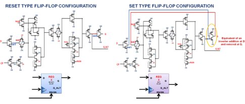
The proposed flip-flop design is an alternative implementation of existing RESET or SET type flip-flop that can be converted into a counterpart equivalent by simple change of pin connection for metal configurability without any addition of new transistor or external logic. The operation is very similar to the second alternative of inverter pair insertion but the only difference here being that instead of insertion we rather reconnect the existing inverters inside the flip-flop itself to change its reset state. While in the conventional solution we need to invert both the input data D as well as output Q for RESET to SET or vice-versa conversion, proposed circuit realizes the same logic modification by removing one internal inverter from the output Q path and adding the same at the input data D as shown in figure 3. This not only resolves the issue of spare inverters but also helps in maintaining same footprint and area for the configurable flop with 3 additional internal contact points.

Figure 3: Using internal inverter substitution over external inverter addition to change flip-flop reset value.
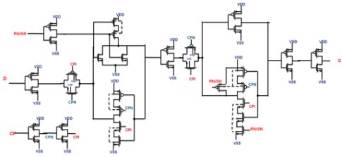
Figure 4 and 5 represent the transistor level schematic that show how a typical asynchronous RESET type flip-flop can be converted into the proposed circuit which can function as either RESET or SET type flop. The proposed circuit therefore is implementable similar to alternative 3 i.e. change of one pin connection of the SET/RESET flop at the point of ECO while its layout is similar to alternative 2 as discussed above. Figure 6 depicts how the proposed circuit layout can help in converting the flop reset value from SET type to RESET type by simply changing two internal interconnects. The difference in the timing upon conversion will thus be seen only due to minor change in setup, hold and clock-to-out time for the modified flop, rest all the design collaterals will be same.
Figure 4: Base conventional asynchronous RESET type flip-flop.
Figure 5: Base proposed asynchronous RESET type flip-flop which can be configured as SET type through contact change.
Figure 6: Abstract layout comparison between reference (conventional) and proposed asynchronous RESET flip-flop circuit.
Table I shows a relative comparison between the various conventional set/reset ECO implementation methods and the proposed configurable solution. It can be observed that the proposed flop if configured to be of RESET type has the same timing, area and power figures as the conventional RESET flop while the configurable conventional SET-RESET flop has a much larger overhead. Additionally, when the proposed flop is converted to SET type, due to a buffer addition at the input data the setup time increases by an inverter delay similar to alternative 2 but clock to out delay is rather reduced by an inverter delay unlike alternative 2. The comparison elucidates that alternative 3 is only best suited for minimum post ECO impact on timing and implementation, however the overhead to enable this configurability throughout the design bears a considerable restriction over the gross power, timing and area since these are not optimum in conventional flop circuit. Furthermore, the comparison also highlights that the timing uncertainty associated with alternatives 1 and 2 is also not easier to manage especially if the concerned path is timing critical as shown in figure 7. In the given figure the ECO (used as an example earlier) implementation shows that there may be a considerable routing as well timing changes when the conventional method is followed by using either or both the alternatives 1 & 2 while no such issue exists in case of the proposed method. Thus, amongst all these solutions the proposed method and circuit seem likely to be a more balanced solution with limited timing impact and no implementation overhead while supporting easier ECO compatibility.
TABLE I: Timing and implementation comparison for proposed and conventional methods in the same technology. (Conversion of RESET to SET type flip-flop).
Click to enlarge

Click to enlarge
Figure 7: Post Silicon Metal Only ECO Implementation using conventional & proposed circuit for down_counter example.
5. Conclusion
There are several other workarounds available for the implementation of different functionalities with the help of same or different configurable cells. Some VLSI designers even use the base/metal configurable larger layout cells which can be transformed from RESET to SET or vice-versa with the changes in the metal/base layers. However, any configurable multi-functionality cell architecture always consumes larger area and power with respect to an independent single functionality cell. The primary challenge is thus to generate an ECO feasibility in physical design with minimal implementation and timing impact. The existing solutions of using available spare cells impact timing as well as routing and thus may create new issues upon implementation. Moreover, since the expected future ECO location is hardly known while implementing the base design, spare cells, whether configurable or not, are of no use if not found in the vicinity. The only solution to resolve such ECOs with minimum design impact is to have a configurable SET/RESET flop. The existing solution for such type of flip-flops has a huge impact on overall design area and power. Therefore, against the conventional solutions, the proposed circuit not only supports the configurability to alter its reset value through a simple change of metal layer but also has similar area, power, foot-print and timing making it much more compatible for in place ECO in physical design and metal only ECOs.
Related Semiconductor IP
- NPU IP Core for Mobile
- NPU IP Core for Edge
- Specialized Video Processing NPU IP
- HYPERBUS™ Memory Controller
- AV1 Video Encoder IP
Related White Papers
- e-GPU: An Open-Source and Configurable RISC-V Graphic Processing Unit for TinyAI Applications
- Reconfiguring Design -> How to extend configurable CPU performance
- SoC Configurable Platforms -> Taking flexibility to the max in platforms
- SoC Configurable Platforms -> Network synchronization relies on CSoC
Latest White Papers
- Breaking the Memory Bandwidth Boundary. GDDR7 IP Design Challenges & Solutions
- Automating NoC Design to Tackle Rising SoC Complexity
- Memory Prefetching Evaluation of Scientific Applications on a Modern HPC Arm-Based Processor
- Nine Compelling Reasons Why Menta eFPGA Is Essential for Achieving True Crypto Agility in Your ASIC or SoC
- CSR Management: Life Beyond Spreadsheets


