AICP: AURA Intelligent Co-processor for Binary Neural Networks
Advanced Computer Architecture Group, Dept. Computer Science, University of York, York, YO10 5DD, UK
(mjf,mweeks,austin)@cs.york.ac.uk
Abstract
AURA (Advanced Uncertain Reasoning Architecture) is a generic family of techniques and implementations intended for high-speed approximate search and match operations on large unstructured datasets. AURA technology is based upon binary Correlation Matrix Memories (CMM). This paper describes a high performance IP-core for executing the core AURA operations. The IP-core processes the AURA data in compact-bit vector (CBV) format, which increases storage capacity but creates issues regarding performance. The IP-core is intended for implementation on the PRESENCE-2 AURA hardware accelerator PCI-card, and for use in SOC and embedded solutions.
1. Introduction
Future ubiquitous and pervasive systems will require a degree of embedded intelligence which will be applied to data processing and interpretation tasks as diverse as speech recognition, video and image processing, and making 'intelligent' decisions about combinations of events detected in the locale of the system deployed. In order to make this possible within an efficient ubiquitous system, this will demand an integrated SOC solution that encompasses dedicated resources, optimised for such data processing tasks, rather than relying upon powerful CPU resources, which may well be unacceptable for such low-power embedded applications. The AICP project seeks to develop an IP-Core based upon the successful AURA technology [Austin, 1995]. This IP-Core will be in two forms, first a scaleable VHDL model for use with FPGA platforms, and second, an IC macrocell for use in true ASIC SOC implementations.
AURA (Advanced Uncertain Reasoning Architecture) technology is intended for high-speed approximate search and match operations on large unstructured datasets. AURA is fast, economical, and offers unique advantages for finding near matches not available with other methods. AURA is based upon a high performance binary neural network called a Correlation Matrix Memory (CMM). AURA finds exact and near matches between indexed records and a given query, where the query itself may have omissions and errors. The degree of nearness required during matching can be varied through thresholding techniques. To support these core CMM computations the PRESENCE (PaRallEl Structured Neural Computing Engine) hardware-accelerator card has been developed.
In this paper, we first introduce the AURA architecture and the PRESENCE accelerator cards. This is followed by a description of an AURA IP core processor, detailing its performance in comparison with the AURA software library. We then close the paper with conclusions and future work.
2. AURA
Binary Correlation Matrix Memories (CMM) are the basis for the AURA technology. CMMs are neural networks for the storage and retrieval of binary vector patterns. Each column of the memory matrix is seen as a neuron, and each row represents an input and synapses to each neuron.
A CMM has two main modes of operation; train and recall. In training mode, a binary output vector (typically representing objects/records) and a binary input vector (representing parameters/features) are associated in the CMM, shown in Figure 1. A recall operation involves applying a query input (or index) vector to the CMM. Each set bit in the input vector selects a row in the CMM, and each set bit in that row is summed into the relevant column counter. The column count provides a score for the degree of closeness of the records to the query. Thresholding can be applied to the column count data to select the best matches. Two types of thresholding can be applied, Willshaw or Lmax, dependent upon the application. Willshaw [Willshaw, 1969], thresholding compares the summed columns with an absolute threshold level, whilst Lmax [Casasent, 1992], retrieves the top L matches from all of the summed columns. A detailed operation of CMM neural networks can be found at [Austin, 1996].
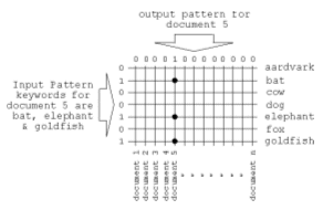
Figure 1 - An example of an inverted index teach
CMM techniques lend themselves for use in such applications as inverted indexes, whereby objects are stored in the CMM, categorised by certain attributes. An example of this is a keyword search of documents, where the output pattern associates one or more bits with a list of documents, and the input pattern describes keywords in the documents. Figure 1 illustrates how documents and keywords are taught into a CMM. A recall operation applies selected keywords as the input pattern, and the column counts of the output pattern indicates matching documents.
AURA is highly scalable, in terms of both processing and storage [Weeks, 2002]. For high performance applications a CMM can be split into vertical stripes and distributed over multiple processing elements, allowing data to be processed in parallel, whilst reducing each element’s storage requirements.
3. PRESENCE HW Platform
The PRESENCE family of hardware architectures has been designed to accelerate CMM operations. As AURA is highly scalable, multiple PRESENCE cards can be combined to create very large CMMs that can be searched very rapidly when compared to software based solutions. The original PRESENCE card was a PCI-based design, that stored and processed CMM data in a binary vector format. This design consisted of a 5-stage pipelined binary neural processor implemented in one time programmable (OTP) FPGAs, with the memory matrix stored in asynchronous DRAM [Moulds, 1999]. Typical AURA applications however use very sparse data sets; hence binary CMM representations can be highly inefficient in terms of storage, and therefore, processing performance.
The latest AURA hardware acceleration card, PRESENCE-2 is shown in Figure 2. This card has greater processing power, storage capacity and interconnection speeds, in a more flexible design [ACAG, 2002]. The main components of the PRESENCE-2 card are shown in Figure 3, these include :
- 3 or 6 million gate Virtex-II FPGA
- Texas instruments TMS6203 DSP
- up to 4 gigabytes of SDRAM
- two 1Mbyte ZBT SRAM memories
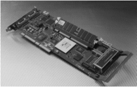
Figure 2 - PRESENCE-2 card
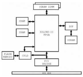
Figure 3 - PRESENCE-2 block diagram
Unlike its first incarnation, PRESENCE-2 is not limited to AURA processing; it has been designed specifically for use with pattern-matching applications such as data mining, biometric recognition, video/audio processing, and is an ideal platform for IP/ASIC prototyping. The card provides for easier and faster development of working systems, whilst system upgrades can be performed with the card in-situ by uploading a new FPGA configuration file into the onboard FLASH memory.
4. AICP IP-Core
The aim of the AICP project is to develop an AURA Compact Binary Vector (CBV) processor IP core for FPGA and ASIC, SOC applications to support CMM operations. The processor core will also include generic CBV vector processing operations in order to make the design more flexible. A CBV representation encodes the ‘1’ bit positions within a binary vector with an integer value, allowing an efficient representation for large sparsely populated binary vectors e.g.
| | Bit position | 9 8 7 6 5 4 3 2 1 0 |
| Binary vector | 0 1 0 0 0 0 0 0 1 1 | |
| CBV | 8,1,0 |
In applications of this type, typically 1 to 10 bits would be set per 1000 bits in the CMM. The length of a CBV is dependent on the data contained within the uncompressed binary vector, therefore, a header record is included with the CBV defining it’s: length, and minimum and maximum set bit positions.
The data contained in a CMM represents the state of the binary neural network and as such does not have any numerical value. Therefore, traditional processor architectures are not optimised to process this type of data. For example, the steps involved in a logical AND operation on three CBVs would be:
- Clear working memory.
- Input pattern selects desired rows in CMM
- Increment memory location indicated by row CBV.
- Willshaw threshold memory at level 3.
This example shows the sequential processing steps that a typical processor would have to perform. Therefore, two FPGA based processor architectures have been developed, designed to increase parallelism, and therefore, performance of CMM operations. These processors are implemented using Xilinx Virtex II FPGAs [Xilinx, 2004], with the processing performance of each benchmarked against a TI DSP and a Pentium 4 based computer. The operation of these new architectures can be categorised as a single instruction, multiple data (SIMD) processor, optimised for CBV data processing.
The first architecture considered is a processor farm [INMOS, 1988], constructed from Xilinx 32bit RISC MicroBlaze processor soft-cores [Xilinx, 2002], increasing CBV processing performance by splitting data across a number of processing nodes. In this architecture a master farmer node dispatches CBV data from external SDRAM to slave worker nodes to be processed, as shown in Figure 4. In this implementation there are four worker nodes. This can be increased dependent on the desired application. The number of processors is limited by the FPGA resources. Each processor requires 225 slices and the more devices added to the system bus reduces its performance by increasing the associated logic delays, therefore, reducing the system’s maximum clock speed. To minimise this problem a hierarchy of processor farms could be constructed, using separate system buses.
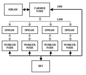
Figure 4 - Processor farm architecture
Each worker node has its own local instruction and data memory connected to the processor via its local memory bus (LMB). In addition to this, it also has two shared memory spaces, one with the farmer node, implemented in internal dual port memory, used to pass data and return results. The other memory space, shared with the worker nodes and farmer node, is implemented in external ZBT (Zero Bus Turnaround) RAM. The ZBT RAM is used as a working memory space, allowing the worker nodes to share the same data set. This memory is connected to each processor via its on-chip peripheral bus (OPB) [IBM, 1999]. The OPB arbiter controls access and collision detection to this memory.
The second architecture considered is a stream co-processor, shown in Figure 5. This processor is highly pipelined with functional units optimised for CBV operations:
- Move : uncompress a CBV to ZBT memory by storing 1 at each CBV index.
- Increment : combine multiple CBVs in ZBT memory by adding 1 to each CBV index.
- Threshold : scan through ZBT memory writing the index of memory locations that are greater than the specified threshold to the output queue.
- ZBT memory controller : initialises ZBT memory to zero and updates tag fields associated with each location indicating if its associated data is valid or can be overwritten.
In this configuration only one functional unit is used at a time. However, this sequential stream operation, achieves almost 100% ZBT memory transfer bandwidth, maximising data processing performance.
The stream co-processor is associated with a MicroBlaze processor, using an OPB interface to access the stream controller. The MicroBlaze processor can then request low-level CBV operations to be performed on selected rows stored in external SDRAM. Data is then transferred from SDRAM in a continuous burst, through the desired pipelined stream functional unit into external ZBT RAM working memory.
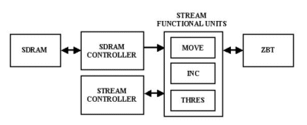
Figure 5 - Stream processor architecture
To improve the performance of both of these architectures, parallelism can be added at different levels. Low-level parallelism is added at the instruction level. Consider the previous example of a logical AND operation performed on three CBVs. The increment and threshold operations can be combined into a single operation. Now during an increment operation a threshold operation can also be performed to see if the result produced on the next cycle will exceed the desired level (Willshaw threshold). If this result is true, the data can be written to a result queue and the working memory tagged to indicate that no further action needs to be taken for this data. This also improves the system’s performance by preventing future write operations to these memory locations, freeing ZBT memory cycles for other operations. A similar low level operation can be performed in the processor farm architecture with one worker node monitoring the results written to the ZBT memory. High level parallelism can be achieved by dividing the CMM into vertical stripes and assigning each block of data to a separate processor i.e. replicating functional units and worker nodes within the FPGA and associating them with separate external ZBT working memory. Assuming that data is evenly spaced across the CMM, high-level parallelism is only limited by:
- Data bandwidth of SDRAM.
- Number of ZBT memory devices
The effect of the first limitation is reduced as most CBV instructions use read-modify-write operations and the CBV data representation is a lot smaller than the SDRAM data width i.e. the SDRAM controller can read 4 to 8 elements of a CBV in one cycle, and that on average a functional unit only requires new data every two cycles.
To assess the initial processing performance of these processor architectures, the increment operation was selected since it is used in a number of CBV operations e.g. AND, OR etc. To allow a true comparison to be made with the TI DSP and the Pentium processor no high level parallelism was included. To bench mark the performance of these processors the following C code was used:
(*(BUFR + *(BUFA + i)))++;
In this simple test code a CBV containing 128 set bit positions is used and repeated 1 to 4 times i.e. a CBV operation with 1 to 4 operands. The results of this test are shown in Figure 6. The performance of the processor farm is relatively flat due to the spare bandwidth within the ZBT memory bus i.e. as more processors are included data latency increases but the overall memory bandwidth is improved. However, owing to collisions on this data bus i.e. two processors accessing the same data, and arbitrations overheads, 100% data transfer bandwidths can not be achieved (actual value dependent on CBV data). Using simulations it was estimated that to obtain the same processing performance as the DSP processor approximately eight worker nodes would be required. From these benchmarks it was concluded that the stream co-processor offered the best overall performance due to its increased ZBT memory bandwidth utilisation and smaller size.
To allow a true comparison of the stream co-processor to be made, the next benchmark is based on a real data set i.e. a data set a lot larger than the processor’s cache. This data is arranged as a CBV CMM with the following characteristics:
| Number of columns: | 500,000 |
| Number of rows: | 60,000 |
| Number of set bits: | 6,805,443 |
| Average set bits per column: | 13.6 |
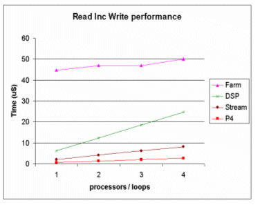
Figure 6 – Initial Benchmark
This large data set allows a true indication of the continuous processing performance of both systems. The software based system was tested on an AMD Athlon XP2000+ with 256M RAM and gave the following results:
Willshaw threshold of 1 = 8.78 ms
Willshaw threshold of 2 = 6.45 ms
Willshaw threshold of 5 = 4.65 ms
Willshaw threshold of 10 = 4.54 ms
The hardware based solution was tested on a Virtex II FPGA running at 133MHz, with no high level parallelism and gave the following results:
Willshaw threshold of (1,2,5,10) = 4.36 ms
From these results, it can be seen that the search time for the FPGA based stream co-processor is independent of the threshold chosen, since the threshold comparison is performed in parallel with the stream functional unit i.e. the processing pipeline is not affected by control hazards. The performance of the stream co-processor system can now be improved by increasing the number of data streams processed in parallel. At present the PRESENCE 2 card can process two parallel data streams (limited by having two ZBT memory ports). An alternative method of increasing processing performance is to increase the system’s clock speed to 225MHz. Combining these methods will give a result of:
| Willshaw(1,2,5,10) = 2.54 ms | 1.78 to 3.45 speedup |
| with two streams = 1.27 ms | 3.5 to 6.9 speedup |
| with four streams = 635 us | 7.1 to 13.8 speedup |
5. Conclusions
In this paper we have shown that new architectures are needed for the efficient handling of CBV-based AURA processing. We have identified a streaming processor architecture that is both efficient and scalable. A single AURA IP core, running on the PRESENCE-2 architecture, compares favourably with the AURA library software running on one of today’s high performance PC architectures. However, in a SOC/embedded environment, the AICP design provides significant performance at low cost and low power. The AICP design is also highly scalable, with the inclusion of additional ZBT SRAM memory ports.
From this version of the AURA IP core a number of areas for possible future work have been identified. These include, improved memory management, minimising overheads associated with the addition or deletion of vectors from CMM and optimising functional units to increase system clock speeds. The next version of the PRESENCE-2 PCI card is also under development, replacing SDRAM with DDR memory modules and adding additional ZBT SRAM memory ports, to increase high level parallelism.
Acknowledgements
The work presented in this paper was supported by the DTI Next Wave Technologies and Markets programme and Cybula Ltd, as part of the AMADEUS virtual research centre [AMADEUS, 2004].
References
ACAG, (2002), AURA - Research into high-performance pattern matching systems
AMADEUS, (2004) AMADEUS website
Austin J., Kennedy J., Lees K., (1995), The advanced uncertain reasoning architecture, Weightless Neural Network Workshop, York..
Austin J., (1996), Distributive associative memories for high speed symbolic reasoning. Int. J. Fuzzy Sets Systems, 82, 223-233.
Casasent D.P., Telfer B.A., (1992), High capacity pattern recognition associative processors. Neural Networks 5(4), 251-261.
IBM, (1999), The CoreConnect™ Bus Architecture
INMOS, (1988) Occam2 Reference Manual, Prentice Hall, ISBN 0-13-629312-3
Moulds A., Pack R., Ulanowski Z., .Austin J., (1999), A high performance binary neural processor for PCI and VME bus-based systems. Weightless Neural Networks Workshop.
Weeks M., Hodge V., Austin J., (July 2002), Scalability of a Distributed Neural Information Retrieval System, 11th IEEE Int. Symposium on High Performance Distributed Computing,.
Willshaw D.J., Buneman O.P., Longuet-Higgins H.C., (1969), Non-holographic associative memory, Nature 222, 960-962.
Xilinx, (August, 2002), MicroBlaze RISC 32bit Soft Processor
Xilinx, (June 2004), Virtex-II Platform FPGAs: Complete Data Sheet, DS031 (v3.3)
Related Semiconductor IP
- NPU IP Core for Mobile
- NPU IP Core for Edge
- Specialized Video Processing NPU IP
- HYPERBUS™ Memory Controller
- AV1 Video Encoder IP
Related White Papers
- Learning how to learn: Toddlers vs. neural networks
- Wind Turbine Fault Detection Using Machine Learning And Neural Networks
- Machines can see, hear and analyze thanks to embedded neural networks
- Pyramid Vector Quantization and Bit Level Sparsity in Weights for Efficient Neural Networks Inference
Latest White Papers
- Breaking the Memory Bandwidth Boundary. GDDR7 IP Design Challenges & Solutions
- Automating NoC Design to Tackle Rising SoC Complexity
- Memory Prefetching Evaluation of Scientific Applications on a Modern HPC Arm-Based Processor
- Nine Compelling Reasons Why Menta eFPGA Is Essential for Achieving True Crypto Agility in Your ASIC or SoC
- CSR Management: Life Beyond Spreadsheets