A Framework for Selection of Cache Configurations for Low Power
IHP GmbH, Im Technologiepark 25
15236 Frankfurt (Oder), Germany
Abstract:
We have described and applied a technique for selection of processor cache configurations for low power using a parameter defined as a product of the cache miss rate and cache size.
1. Introduction
Powerful embedded processors are crucial for competitive System-on-Chip (SoC) solutions. SoC strongly request both energy saving and high speed processing to enable flexible and fast adaptable designs.
Therefore, a processor that can be configured according to the requirements of various application fields is needed. Configurations can include one or more coprocessors, one or more caches, scratchpad memory, on-chip trace memory, on-chip buses, etc. Usually, the highest attention is paid to configuring caches. The configuration process supposes making decision on the size, associativity and organisation of the instruction and data cache. To select appropriate configurations and choose the power-optimal one for specific application field is a difficult task [1-6].
In this paper, we describe a simple framework for selection of MIPS processor cache configurations for low power on the basis of cache miss rates and implementation details. The paper is organised in four sections excluding the introduction and conclusion: Section 2 shortly describes features of the MIPS 4KEp processor core. Section 3 presents C-applications relevant for selection of the cache configurations. The cache configurations are analysed in Section 4. Implementation and verification details of the optimal cache configuration are presented in Section 5.
2. MIPS Core
The 4KEp™ core implements the MIPS32™ architecture with the Memory Management Unit (MMU) interfacing between the Execution Unit and the Cache Controller. This core provides a simple Fixed Mapping Translation (FMT) mechanism. It performs virtual to physical address translation and provides attributes for the mapped regions. The block diagram of the core is shown in Figure 1.
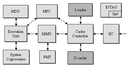
Figure 1: Block diagram of MIPS 4KEp core [7]
The Master Pipeline Control (MPC) is responsible for recognising and managing dependencies in the pipeline. This involves decoding each instruction and checking to see if there are interlocks that need to block the issue of the next instruction. The Execution Unit implements the fundamental 32-bit integer data manipulation functions. In addition to data calculations, it contains logic for branch determination, branch target calculation, and the load aligner. To conserve area, the 4KEp core uses an area-efficient iterative Multiply-Divide Unit (MDU). Multiplier performs an iterative one-bit shift-add every cycle. Multiplies are completed in 32 clock cycles. Multiply accumulates and multiply subtracts take additional two cycles to do the final accumulate step. Divides are also iterative, but do not have the data-dependent early-in optimisation. The System Coprocessor supports the virtual memory system and exception handling.
The EC interface contains the logic to drive the external interface signals. Additionally, it contains implementation of the 32-byte collapsing write buffer. The purpose of this buffer is to store and combine the write transactions before issuing them at the external interface.
An optional Enhanced JTAG (EJTAG) block allows for single-stepping of the processor as well as instruction and data virtual address breakpoints.
Instruction and data caches are fully configurable from 0-64 KB in size. In addition, each cache can be organised as direct-mapped or 2-way, 3-way, or 4-way set associative. Caches are virtually indexed and physically tagged to allow them to be accessed in the same clock that the address is translated.
3. Applications
We have selected three C-applications. First program is the AES (Advanced Encryption Standard) symmetric block cipher [8]. This program is an optimised version implemented by Vincent Rijmen [9]. Next two programs are implementing well-known RSA asymmetric encryption and decryption algorithms [10]. RSA is working with two different keys: public key Kpublic = (n,e), which can have everybody and private key Kprivate = (n,d), which is known only to owner. Here n and d are big numbers (1024 bits) and e, called public exponent, can be 3, 17 or 216+1. The encryption process is described by:
The decryption can be performed using the expression:
Two encryption algorithms (AES and RSA) are usually applied in sequence in wireless technology for data exchange. These algorithms and programs based on them are completly different in structure. At first a key is generated for AES, then RSA encryption is executed. Finally, the AES-key can be used for encryption of large data.
The RSA asymmetric encryption and decryption algorithms are used for the protected key-exchange of symmetric algorithms.
4. Cache Configurations
Choosing a cache size involves balancing the conflicting requirements of area and miss rate. If the cache line size is increased, then the miss rate is reduced. If the number of cache lines is increased, then the miss rate can be reduced if the tiling size or the degree of set associativity is also increased. Since there is a limit to the cache size, performance tradeoffs have to be investigated.
In cache synthesis, it is necessary to analyse the power dissipation for cache of various sizes and associativities. There are several models for estimation of the power consumption of a cache [11-13]. These models are based on estimation of the energy dissipation of one cache access for a certain cache size and configuration.
When SRAM cache is accessed, its energy consumption mainly comes from the switching capacitance. The total switching capacitance for each cache access is directly dependent on the configuration of a cache (size, block size, associativity, etc). On other hand, a cache consumes energy proportionally to the number of accesses, which in turn can be hits or misses. The energy components of an instruction cache are read hit energy and read miss energy. Taking into account writing operations, the energy components of a data cache are: read hit energy, read miss energy, write through energy, and write around energy.
As the cache miss energy is much higher than the other energy components, we use the cache miss rate to define a parameter (called Power Index) that gives us the opportunity to evaluate different cache configurations according to the power consumption and cache size. Namely, Power Index is defined as a product of the cache miss rate and the normalised cache size (it is the size of a cache multiplied by 10 KB-1):
The Power Index model implies the existence of a tradeoff relation between the cache miss rate and cache size. Namely, the power consumption has a sweet spot as cache size changes: for a too small cache, program thrashes burning power on external memory accesses; for a too large cache, cache itself burns too much power. As miss rate decreases with increase of the cache size, their product must have a local minimum for given application. In other words, there must be an optimal point between them.
Applications described in Section 3 are used to investigate application dependencies of miss rates of both instruction and data cache. Table 1 and Table 2 show the miss rates of instruction and data caches of different size and associativity. Higher associativity (the number of ways) reduces the miss rate [14] but needs more LRU and dirty bits in a Way-Select RAM array. To trade-off between these two contradictory demands, we have decided not to exceed the associativity of 2. Presented results are obtained executing the programs on the Green Hills instruction set simulator of the MIPS 4KEp core.
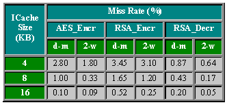
Table 1: Instruction Cache Miss Rate
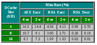
Table 2: Data Cache Miss Rate
Now we simply can calculate Power Index for different applications and cache configurations. The results are presented in Table 3 and Table 4.
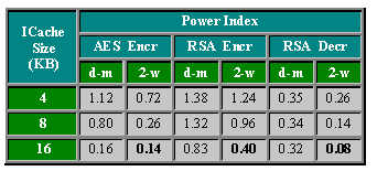
Table 3: Instruction Cache Power Index
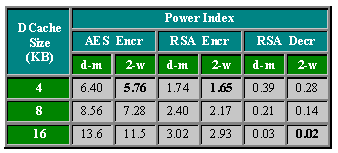
Table 4: Data Cache Power Index
Selection of candidates for the optimal cache configuration starts with the identification of all configurations with the lowest Power Index. Of course, the cache miss rate is 0 in an ideal case when the cache size is equal to the external memory size. According to the values of Power Index in Table 3 and Table 4, the optimal cache configuration for given combination of applications is as follow: Instruction Cache of 16 KB size and 2 ways (the lowest Power Index for each of three applications) and Data Cache of 4 KB size and 2 ways (the lowest Power Index for two of three applications).
5. Implementation and Verification
Instruction and data cache RAM organisations for the optimal cache configuration are presented in Table 5. Functional Verilog SRAM model including timing information has been used for description of Tag and Data RAM arrays of both instruction and data cache. Way-Select RAM arrays have been made of flip-flops. To increase testability, we have implemented the integrated memory BIST. The implemented design is verified in the functional verification environment for a MIPS core.
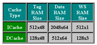
Table 5: Organisation of the optimal cache configuration
In the IHP’s 0.25µm CMOS technology having 5 metal layers, the core area (including the WS arrays of caches) is 5.7 mm2. The core integrates about 67000 NAND gates (about 268000 transistors). Estimated power consumption is 500 mW at the operating frequency of 70 MHz.
6. Conclusion
We have defined Power Index for evaluation of the cache power consumption on the basis of cache miss rate and size, and described the technique for selection of cache configurations for low power.
As expected, the optimal instruction cache configuration is the one of maximal size and maximal associativity. On the contrary, the optimal data cache configuration in this case is the one of minimal size and maximal associativity.
Further work will be in direction of exploring the effect of block size and higher associativity on Power Index of a processor cache.
References
- T. Givargis, F. Vahid, and J. Henkel, “System-level exploration for Pareto-optimal configurations in parameterized SoC,” IEEE Trans on VLSI Systems, Vol.10, pp.416-422, Dec. 2002.
- A. Malik, B. Moyer, and D. Cermak, “A programmable unified cache architecture for embedded applications,” Proc. Int. Conf. on Compilers, Architecture, and Synthesis for Embedded Systems, Grenoble, July 2000.
- D. H. Albonesi, “Selective cache ways: On-demand cache resource allocation,” 32nd Annual International Symposium on Microarchitecture, Haifa, Nov. 1999.
- W. T. Shiue and C. Chakrabarti, “Memory exploration for low power embedded systems,” Proc. Design Automation Conference, New Orleans, June 1999.
- Y. Li, W. Wolf, and J. Henkel, “Tasklevel memory hierarchy synthesis for low power realtime systems,” 6th International Workshop on Hardware/Software Co-Design, Seattle, March 1998.
- P. R. Panda, N. D. Dutt, and A. Nicolau, “Data cache sizing for embedded processor applications,” Proc. DATE Conference, Paris, Feb. 1998, (pp.925-926)
- http://www.mips.com/content/Products/
- http://csrc.nist.gov/CryptoToolkit/aes/
- http://www.esat.kuleuven.ac.be/~rijmen/
- http://indigo.ie/~mscott/
- K. Itoh, K. Sasaki, and Y. Nakagome, “Trends in low-power RAM circuit technologies,” Proceedings of the IEEE, Vol.83, pp.524 -543, April 1995.
- M. B. Kamble and K. Ghose, “Analytical energy dissipation models for low power caches,” Proc. Symposium on Low Power Electronics and Design, August 1997, (pp.143-148)
- Y. Li and J. Henkel, “A framework for estimating and minimizing energy dissipation of embedded HW/SW systems,” Proc. Design Automation Conference, San Francisco, June 1998, (pp.188-193)
- J. Hennessy and D. Patterson, Computer architecture: A quantitative approach, Morgan Kaufmann Publish., Third Edition, 2003.
Related Semiconductor IP
- oFEC Encoder and Decoder
- NPU IP Core for Edge
- NPU IP Core for Mobile
- NPU IP Core for Data Center
- NPU IP Core for Automotive
Related White Papers
- Right Python Framework Selection for Automation Testing
- Selection of FPGAs and GPUs for AI Based Applications
- Design and implementation of a hardened cryptographic coprocessor for a RISC-V 128-bit core
- Customizing a Large Language Model for VHDL Design of High-Performance Microprocessors
Latest White Papers
- Customizing a Large Language Model for VHDL Design of High-Performance Microprocessors
- CFET Beyond 3 nm: SRAM Reliability under Design-Time and Run-Time Variability
- Boosting RISC-V SoC performance for AI and ML applications
- e-GPU: An Open-Source and Configurable RISC-V Graphic Processing Unit for TinyAI Applications
- How to design secure SoCs, Part II: Key Management