A Flexible 200kHz-20MHz Ring Oscillator in a 40nm CMOS Technology
Murilo P. Pessatti, Pedro A. Zamuner, Alexandre Dal Fabbro, Elton R. Moutinho, Luis H. Spiller, William Prodanov, Joaquin Aguilera, Paulo A. Dal Fabbro (Chipus Microelectronics)
Abstract :
Analog IPs are developed to meet a set of specific requirements, and to change its specifications for a different application, a significant amount of time and effort may have to be applied on customization and redesign. Companies designing analog and mixed-signal SoCs often resort to 3rd party IP companies to reduce time-tomarket, risk or due to lack of expertise in a specific domain. However, most of the times, there is no exact match in the market for an analog IP that would fit perfectly in the SoC. Hence, some level of customization must be carried out by the IP provider in order to fulfill their customer needs.
In this paper, we present a flexible ring oscillator IP designed for a 40nm CMOS technology, whose oscillation frequency can be chosen from 200kHz to 20MHz. It was developed using a new design approach, in which analog IPs are designed from scratch to be flexible, employing modular blocks that can be easily customized. The IP is silicon proven. It works with a supply voltage of 1.2V and features 5% frequency accuracy, occupying an area of 0.0022mm2.
To provide this flexible solution, during the design phase, an exploration of the design space is carried out for the chosen circuit architecture, in this case a ring oscillator. Within the boundaries of the block capabilities, we analyze which parameters must be flexible to the user and assure that performance under process variations, power and area are met. Layout modularization is employed to make it easier to add/remove features. An HDL model is provided together with the IP datasheet once the user has chosen its parameters through a Web interface. This allows the system architect to quickly verify if the IP fits his/her needs, thereby speeding up the SoC development.
I – INTRODUCTION
Oscillators are basic building blocks for integrated circuit (IC) design. The architecture and specification of such blocks can vary according to the application that they are intended for. Within a traditional strategy, regular or low power design equations are first used to choose a typical operating point where the circuit is required to function most of the time, then specific device sizes are changed and extra components are added to fulfill the performance requirements. This approach typically consume time and resources that most of times must be spent again if the block must be customized according to a particular customer requirement. Deviations from the desired performance are diminished by manual and time-consuming iterations where particular sections of the circuits are modified, added or even deleted to improve the specifications, falling into a cumbersome process. This process leads to increased risk and development time.
To avoid this, analog IC designers can use optimization tools to verify and improve their designs, thus saving time and allowing for new ways to boost specifications and parameters to achieve, as they make decisions about architecture and system characteristics. A complete understanding of the software and its benefits to align with the traditional strategy, must be done by the designers so real exploitation of the tools can happen.
To provide a flexible solution, we present a silicon proven IP that works with a supply voltage of 1.2V and features 5% frequency accuracy, occupying an area of 0.0022mm2. Likewise, a web interface is available for the customer to select between a range of IP specifications. The web application will then collect the provided input parameters and produce as an output the closest IP configuration, according to the IP design information available beforehand. In Section II, the flexible design approach is described and we explain how it becomes feasible to achieve flexibility by trading it off with other IP parameter. Following, in Section III, the example and details of the design of a ring oscillator are shown highlighting its flexibility in terms of output frequency and the trade-offs made. An example of the web interface and how the customer can interact with the IP is briefly explained. In Section IV, the simulation and experimental results are revealed and an analysis is conducted on the different variations and parameters. Finally, Section V delivers the conclusion and a brief summary of relevant information.
II – FLEXIBLE ANALOG IP DESIGN APPROACH
A key characteristic of our flexible design approach is that the block is built to be flexible from scratch. The following characteristics makes it unique when compared to a traditional IP design approach:
- Design space
- The flexible approach initiates with an exploration of the design space for the chosen circuit architecture. The parameters that will be flexible and their configuration range are carefully chosen. The design space is limited.
- Not a synthesis
- No automatic synthesis is made.
- IPs designed to be flexible
- Instead of optimizing the IP to be best in class for a particular specification, the design is conducted with flexibility as a priority. Hence, a trade-off must allways be made, which can be be paid in terms of area, current consumption or any another parameter, depending on the type of the IP. The main advantages for the customer are reduced time-to-market and risk.
- VerilogA models
- Once the customer has chosen the IP parameters that fit his/her requirements, he/she can immediately download the corresponding VerilogA model and plug into his/her system level simulation and check if the desired performance and functionality are met.
- Modular layout
- Whenever possible, the IP is built with modular sub-blocks making it easy to add or remove features.
In the next section, we present a ring oscillator designed with this flexible approach.
III – FLEXBILE RING OSCILLATOR
The block diagram of a ring oscillator is shown in Fig. 1. It is composed basically of a chain of inverters with the output connected to the input forming a ring. This ring is biased by a constant current and its output goes through a level shifter so that the supply domain for the oscillating output signal (osc_o) is shifted from lvdd to vdd.
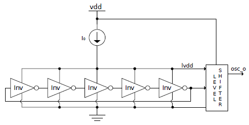
Fig. 1 - Ring oscillator block diagram.
The frequency behavior of such current-controlled ring oscillator is described by (1) [1].
![]()
where fosc is the output frequency of the ring oscillator, Iavg is the average current supplying the ring, N is the number of inverters used in the ring, lvdd is the voltage supplying the ring, and Ctot is the sum of the inverter's input and output capacitances.
Theoretically, according to [1], there is a linear relationship between the output frequency and the ring oscillator supply current. If the approach used to obtain a large range (two decades in our case) of oscillation frequency is only to vary this supply current, which can be controlled by a programmable current mirror to process the input bias current before delivering to the ring circuit, and keeping the other parameters in the equation constant, it will be necessary a large range of supply current. In other words, if the circuit is designed for a high output frequency, then, to achieve a low frequency, the required supply current will be impracticably low. Conversely, if the circuit is designed for a low output frequency, then, for a high output frequency, the current consumption will be excessively high.
One of the problems of this high dynamic range is the circuital complexity of the current mirror to generate this large range of currents. In order to avoid too much mismatch in the transistors in the mirror, it will be necessary to keep the current multiplication rate relatively low and this will require the use of various mirroring stages. These mirror stages will add various current branches that can increase the current consumption for a part of the circuit that is only auxiliary.
Another problem with this large range is because the output of the current mirror will drive the same ring oscillator, which will represent a relatively constant load, and the voltage between the ring oscillator an the current mirror will vary with the variation of the current. If the current is too high, this voltage can be high enough that the transistors in the mirror will leave the saturation region, and if it is too low the output signal of the ring oscillator can be small enough that the design of the level shifter after the ring will be very challenging. In order to avoid those issues described above, as well as the high current consumption at high frequencies, it is possible to obtain a large range output frequency without having a large range of supply current if another parameter in the equation is taken into account. The lvdd parameter is actually a consequence of the value of Iavg and the equivalent resistance of the inverters. The N and Ctot parameters are controllable, but only the Ctot was chosen to be used in the design as a variable.
Figure 2a) shows a first-order representation of the frequency/current relationship of the ring oscillator according to (1) and considering that the other parameters are constant. The linear behavior here is only theoretical because the value of lvdd changes with the variation of the current, so the real behavior will be more non-linear. Figure 2b) represent the same relationship, but now using four different values of Ctot. Comparing these two figures, it is possible to find a combination of Ctot values in a way that covers the same desired frequency range but using a smaller current range.
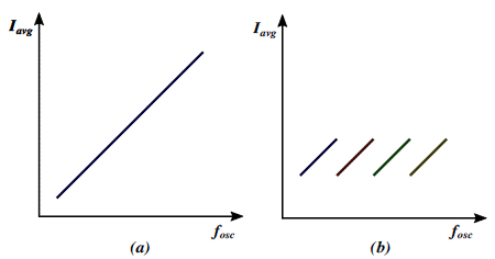
Fig. 2 - Approaches for achieving a high frequency range in ring oscillator: a) varying only the supply current; b) varying the supply current and the capacitance.
The approach used in the design to make the variation of the Ctot parameter possible was to add a set of capacitors for each inverter inside the ring and making the connection of them with each inverter by metal change in layout.
For the testchip, we have instantiated an oscillator for each value of Ctot and each of them covers a certain region of the frequency range. In the design, we have actually allowed some overlaps between the frequency regions to deal with the non-linearities of the relationship between frequency and current and to avoid dead zones in all corner cases.
For each oscillator the same range of supply current is available to use to configure it. The current mirror that allows this configuration was divided in two main parts: the mirror responsible for the selection of the current value that will go to the ring, and the mirror responsible for process trimming adjustment. The first mirror is programmable and is used alongside each oscillator to determine its output frequency. All those combination results, as the output frequency, the current consumption, duty cycle and process trimming adjustment range will be collected for further use.
The idea is that the costumer enters the desired oscillator frequency, from a predefined range, and, in the background, the web application will search in the results table for the closest match and return to the costumer the other specifications for this selected version of the oscillator, together with a VerilogA model. Once the customer approves the specification, the IP, which is silicon proven, is ready to be delivered, including its GDSII file. Figure 3 shows an example of the web interface that allows the customer interaction.
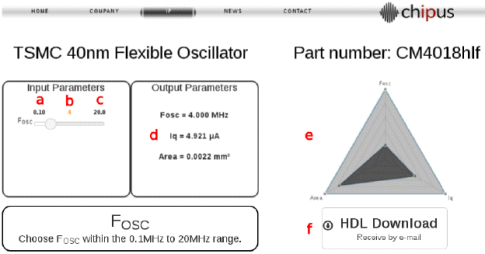
Fig. 3 – Ring oscillator web interface provided to the customer.
(a) Minimum flexible oscillator frequency. (b) Current selected frequency value. (c) Maximum flexible oscillator frequency. (d) Estimated output measurements based on simulation. (e) A dynamic chart for visualization of the output parameters in function of the input frequency. (f) A button to download the HDL model with the current IP configuration.
The web interface enables the customer to interact with the IP input parameters, returning as output parameters the flexible configurations available for the oscillator.
IV – SIMULATION AND EXPERIMENTAL RESULTS
The flexible oscillator was designed and implemented in a 40nm CMOS technology, having as constraints a supply voltage of 1.2V and a bias current of 1μA. Figure 4 shows the simulation results for the output frequency and inverter chain current. It can be seen from this figure that the strategy of using the total capacitance together with the variation of the bias current allowed us to obtain a frequency range from 200kHz to 20MHz with a current consumption that is constrained to a maximum of 10μA.
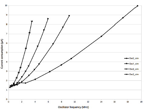
Fig. 4 - Simulation results for the oscillator frequency and current consumption.
The drawbacks for achieving this level of flexibility is that the resulting power consumption and die area are not optimized for a given output frequency. In the flexible design approach for the ring oscillator, our decision was to keep the area constant and make the configuration possible by only changing one metal layer. In order to illustrate this trade-off among output frequency flexibility, current consumption, and die area, Table 1 presents the results for the ring oscillator designed using the flexible (simulated) and the regular (estimated) approaches for three selected frequencies: 200kHz, 10MHz, and 20MHz.
Table 1 - Comparison between flexible and regular oscillator.

As shown in Table 1, using the regular approach and optimizing the oscillator for the desired frequency, 15% can be saved in die area for the 200kHz oscillator, 50% for the 10MHz and 45% for the 20MHz. In terms of current consumption, the 200kHz oscillator is already optimized in the flexible design and would have no benefit from adopting a regular approach. For the 10MHz and 20MHz cases, we estimate a reduction of 17% and 30%, respectively. Hence, a clear trade-off is made and to allow flexibility in terms of output frequency, we had to sacrifice die area and current consumption. The impact of the increase of current consumption has to be analyzed together with the other blocks that will compose the final IC and also current consumption specifications for it. As this oscillator was not intended to be low-power, then this increase is most probably acceptable. The increase in area, by its turn, will represent a relative increase of about 0.1% in the total IC area, if, for instance, we consider that the final IC will ocuppy an area of 1mm2. Therefore, the increase in area is negligible.
Figure 5 shows the experimental results obtained for 10 samples of the ring oscillator. The results presented are the mean of the values measured. The figure shows the same distribution of the one obtained by simulation. The differences observed in the values of currents measured for each frequency are mainly due to the fact that the current reference that bias the ring oscillator was not trimmed.
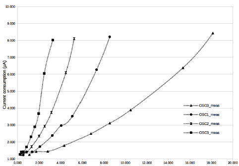
Fig. 5 - Measurement results for output frequency and current consumption for 10 samples of the ring oscillator.
V – CONCLUSION
Flexibility on analog IPs has become crucial to meet today’s aggressive performance and time-to-market requirements. Modular and configurable blocks become a key part in this as they allow to add or remove features and adjust important IP parameters. Likewise, automation is being used to alleviate IP design as it tends to make the IC design engineers more productive and able to tackle harder problems distributing better the resources. It becomes possible to better understand the limits of a certain architecture as well as to deal with trade-offs in a more efficient way.
In this article we presented a 20kHz-20MHz ring oscillator designed, fabricated and tested in a 40nm CMOS technology. For this kind of circuit, there is an obvious trade-off between output frequency and power consumption and in order to increase the first, the consumption is also increased. We explained our flexible design approach, in which is possible to generate an IP semi-automatically. Using a web interface, the customer can chose the output frequency of the oscillator withing a pre-defined range. The web application returns the other parameters and VerilogA model that can be downloaded and plugged into a system level simulation so that the desired performance and functionality can be checked.
We have shown that besides the normal frequency/current trade-off, our flexible ring oscillator approach may further increase the current consumption when compared to a regular design and also the die area. However, the trade-off to be analyzed in this case must be regarding the customer viewpoint, which will be trading higher current consumption and neglible die area increase for readily available semi-customized IP and low risk due to its silicon proven state.
REFERENCES
[1] R.J. Baker, CMOS: “Circuit Design, Layout, and Simulation,” IEEE Press Series on Microelectronic Systems, 3rd Edtion, 2010.
Related Semiconductor IP
- OSC Ring Oscillator Programmable Nano Power Series
- OSC Ring Oscillator Programmable Nano Power Series
- OSC Ring Oscillator Programmable Compensated Series
- Ring oscillator, 100-400MHz - GlobalFoundries 130nm RFSOI
- Ring oscillator, 100-400MHz - GlobalFoundries 130nm RFSOI
Related Articles
- A 66-mW 3.4Gbps Transmitter PHY for HDMI Applications in 2.5V 40-nm CMOS
- Technologist backs low-voltage CMOS for SoC devices
- Tailoring is critical to successful RF analog CMOS chips
- A bluetooth radio in 0.18um CMOS
Latest Articles
- Enabling RISC-V Vector Code Generation in MLIR through Custom xDSL Lowerings
- A Scalable Open-Source QEC System with Sub-Microsecond Decoding-Feedback Latency
- SNAP-V: A RISC-V SoC with Configurable Neuromorphic Acceleration for Small-Scale Spiking Neural Networks
- An FPGA Implementation of Displacement Vector Search for Intra Pattern Copy in JPEG XS
- A Persistent-State Dataflow Accelerator for Memory-Bound Linear Attention Decode on FPGA