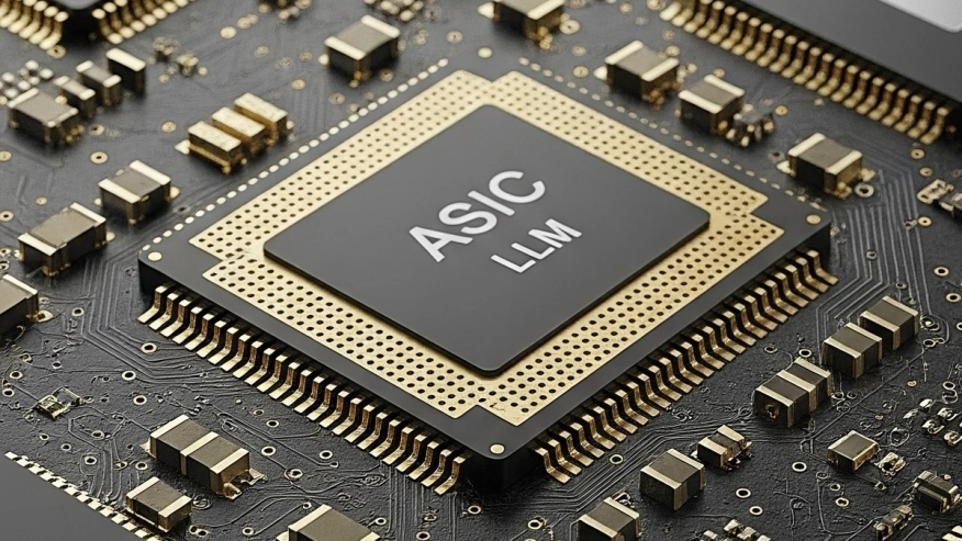
Why ASIC Design Makes Sense for LLM-On-Device
A look at architectural and design considerations when designing ASICs for LLM-on-device.
By Steve Xu, Co-Founder and Chief Architect, XgenSilicon
EETimes | July 14, 2025
Multimodality LLMs can enable powerful real-time vision and audio applications if chip power and cost meet the constraints of edge devices. By adopting an ASIC approach, it’s possible to achieve a hardware-efficient implementation through custom design, resulting in lower power and cost compared to using off-the-shelf components, such as GPUs, NPUs, and application processors.
An ASIC design is a systematic approach to address power efficiency bottlenecks, which may be different from model to model and per deployment constraint.
For example, the power of Snapdragon AR1+ Gen 1 running a 1B vision model is 1 watt. An ASIC implementation of the same model can reduce it to 0.1 watt with design tradeoffs between silicon die area and power consumption by shifting the design from NPU + DDR architecture to ASIC + on-chip memory architecture. For smart glasses with a 500 mAh battery, this translates the active time of vision from 0.5 hours to 5 hours.
In this article, we’ll illustrate architectural and design considerations to be taken into account when planning and designing ASICs for LLM-on-device.
To read the full article, click here
Related Semiconductor IP
- UCIe D2D Adapter & PHY Integrated IP
- Low Dropout (LDO) Regulator
- 16-Bit xSPI PSRAM PHY
- MIPI CSI-2 CSE2 Security Module
- ASIL B Compliant MIPI CSI-2 CSE2 Security Module
Related News
- Why the Microsemi-Actel deal makes complete sense
- Analysis: Why ARM-AMD makes sense
- Cadence-Mentor deal makes sense, says analyst
- Analyst: AMD-ARM deal makes no sense
Latest News
- Wind River Joins the CHERI Alliance and Collaborates with Innovate UK to Accelerate Cybersecurity Innovation
- Arteris and MIPS Partner to Accelerate Development for Physical AI Platforms
- DCD-SEMI expands CryptOne with EdDSA Curve25519 IP core for secure embedded systems
- Syntacore's SCR RISC-V IP Now Supports Zephyr 4.3
- Xylon Presents New 12-Channel GMSL3/GMSL2 FMC+ ExpansionBoard