Aldec Enters the ASIC Prototyping Market with HES-7
Leveraging Xilinx’s Virtex®-7 FPGA, Aldec’s HES-7 expands up to 96m ASIC gate capacity
Banbury, United Kingdom – September 17, 2012 - Aldec Europe is pleased to announce the immediate availability of HES-7, an FPGA-based ASIC/SoC prototyping system that provides hardware verification and software verification teams with a versatile solution; and which lowers the cost of the prototyping process.
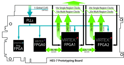
HES-7 takes full advantage of the Xilinx® Virtex-7 2000T 3D IC, which affords a design capacity of up to 24 million ASIC gates on a single, dual-device HES-7 board. In addition, the system employs a non-proprietary high-speed backplane connector that enables easy expansion of custom daughter boards or which can facilitate the connection of up to four HES-7 boards, delivering a total design capacity of up to 96 million ASIC gates.
Zibi Zalewski, Hardware Division General Manager at Aldec, comments: “Prototyping is beneficial to the whole ASIC delivery process, and the most common way to prototype is to use FPGAs. However, with most ASIC designs being between 10 and 20 million gates, to date it has been necessary to employ several low-density FPGAs on a single prototyping board; and implementing the SoC/ASIC design has been a painful and costly process because the design needs to be partitioned between the multiple devices. Using a dual-chip HES-7 prototyping solution from Aldec, equipped with Xilinx’s industry-leading Virtex-7 2000T devices, reduces the design implementation effort and lowers the tool expense when supporting multi-million gate SoC designs.”
Kirk Saban, Sr. Product Line Manager, Virtex-7 Xilinx, added: “The HES-7 product fully leverages the power of our Virtex-7 2000T devices and our Vivado™ Design Suite, which together offer a strong combination of technology that accelerates time-to-validation and drives down the cost of the ASIC prototype process.”
HES-7 is available in four different board configurations, which afford capacities of between 4 and 96 million ASIC gates, and comes with an industry-leading 1 year limited warranty. HES-7 prices start at $19,995.00. For further information, interested parties should visit www.aldec.com/products/HES-7. In addition, a HES-7 ASIC Prototyping white paper is available for download from www.aldec.com.
About Aldec
Aldec Inc., headquartered in Henderson, Nevada, is an industry leader in Electronic Design Verification and offers a patented technology suite including: RTL Design, RTL Simulators, Hardware-Assisted Verification, Design Rule Checking, IP Cores, DO-254 Functional Verification and Military/Aerospace solutions. www.aldec.com
Related Semiconductor IP
- UCIe D2D Adapter & PHY Integrated IP
- Low Dropout (LDO) Regulator
- 16-Bit xSPI PSRAM PHY
- ASIL B Compliant MIPI CSI-2 CSE2 Security Module
- SHA-256 Secure Hash Algorithm IP Core
Related News
- Aldec unveils Xilinx UltraScale FPGA-based prototyping board enabling Simulation Acceleration and Emulation with the latest release of HES-DVM
- Aldec Launches HES-DVM Proto "Cloud Edition" - Giving Engineers Easier Access to FPGA-based ASIC & SoC Prototyping
- Aldec Verifies Compatibility of Northwest Logic's PCI Express Cores with HES-7 SoC/ASIC Prototyping Platform
- Aldec Announces HES-7, the Largest Off-The-Shelf Xilinx Virtex-7 FPGA Prototyping System at up to 288 Million ASIC Gates Capacity
Latest News
- EU DARE Project Is Scrambling to Replace Codasip
- Sofics and Alcyon Photonics Partner to Support Next-Generation Photonic Systems
- QuickLogic Appoints Quantum Leap Solutions as Authorized Sales Representative
- Cadence and NVIDIA Expand Partnership to Reinvent Engineering for the Age of AI and Accelerated Computing
- Cadence and Google Collaborate to Scale AI-Driven Chip Design with ChipStack AI Super Agent on Google Cloud