SDRAM Controller IP
Filter
Compare
239
IP
from
31
vendors
(1
-
10)
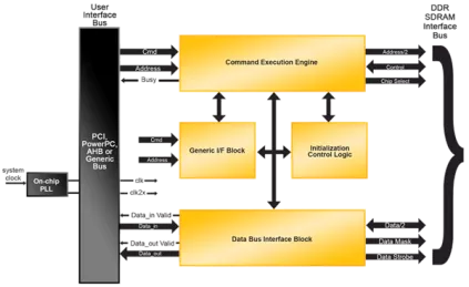
-
AMBA AHB Bus to DDR SDRAM Controller
- External pin reduction by transferring 2 bits of data per pin.
- Supports multiple external SDRAM banks.
- Automatic refresh generation with programmable refresh intervals.
- Self-refresh mode to reduce system power consumption.
- Standard delay cells or user provided DLL for DQ and DQS alignment.
-
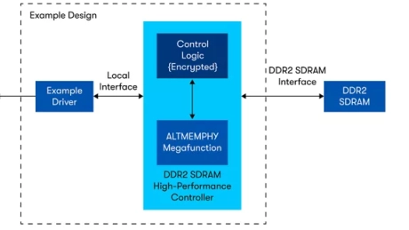
DDR and DDR2 SDRAM Controller with ALTMEMPHY Intel® FPGA IP
- The DDR and DDR2 SDRAM Controller with ALTMEMPHY Intel FPGA Intellectual Property (IP) provides simplified interfaces to industry-standard DDR SDRAM and DDR2 SDRAM
- The DDR and DDR2 SDRAM Controller with ALTMEMPHY Intel FPGA IP core work in conjunction with the ALTMEMPHY physical interface IP function
- The controllers offer a half-rate interface and a full-rate interface to the customer application logic
- For exact device support, please refer to the user guide.
-
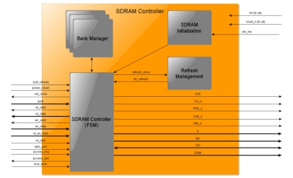
DDR and DDR2 SDRAM Controller Intel® FPGA IP Core
- The DDR and DDR2 SDRAM controllers handle the complex aspects of using DDR and DDR2 SDRAM—initializing the memory devices, managing SDRAM banks, and keeping the devices refreshed at appropriate intervals
- The controllers translate read-and-write requests from the local interface into all the necessary SDRAM command signals.
-
SDRAM Controller DO-254 IP Core
- The SDRAM Controller implements a controller for Single Data Rate Synchronous Dynamic Random Access Memory (SDR SDRAM) devices as specified in the JEDEC Standard No. 21-C Page 3.11.5.1 Release 12.
- Single Data Rate SDRAM can accept one command and transfer one word of data per clock cycle.
-
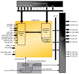
LPDDR3 SDRAM Controller
- Interfaces to Industry Standard LPDDR3 SDRAM components and modules compliant with the JESD-209.3 specification
- High-Performance LPDDR3 performance, up to 400 MHz/800 Mbps operation
- Supports automatic LPDDR3 SDRAM initialization and refresh
- Supports Deep Power Down Mode
-
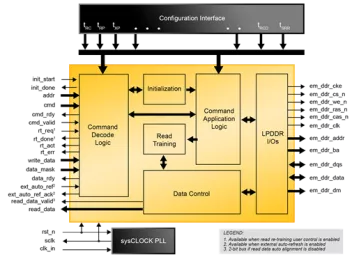
LPDDR SDRAM Controller
- Interfaces to industry standard LPDDR SDRAM according to JESD209B
- Double-data rate architecture; two data transfers per clock cycle
- Bi-directional data strobe per byte of data (DQS)
- Programmable auto refresh support
-
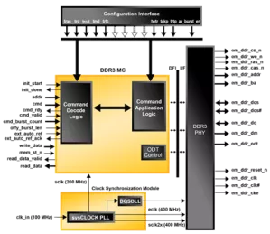
DDR3 SDRAM Controller
- Support for all LatticeECP3 “EA” devices
- Interfaces to Industry Standard DDR3 SDRAM components and modules compliant with JESD79-3, DDR3 SDRAM Standard
- Interfaces to DDR3 SDRAM at speeds up to 400 MHz / 800 Mbps in -8 speed grade devices
- Supports memory data path widths of -8, -16, -24, -32, -40, -48, -56, -64 and -72 bits
-
-
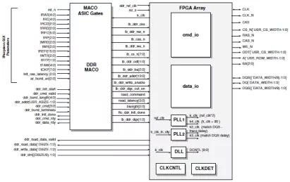
DDR SDRAM Controller - Pipelined for ispXPGA and ORCA4
- Performance of Greater than 100MHz (200 DDR)
- Interfaces to JEDEC Standard DDR SDRAMs
- Supports DDR SDRAM Data Widths of 16, 32 and 64 Bits
- Supports up to 8 External Memory Banks