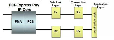
PCI Express 3.1 IP
Filter
Compare
317
IP
from
16
vendors
(1
-
10)
-
Multi-Port Switch IP for PCI Express
- Designed according to the PCI Express 4.0, 3.1, 2.1, and 1.1 specifications, including the latest errata
- Designed according to the PCI-SIG Single-Root I/O Virtualization specification
- Supports PIPE PHY interface definition including variable clock and variable data
- Supports 16.0, 8.0, 5.0 and 2.5 Gbps line rates
-
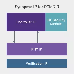
IDE Security IP Modules for PCI Express 7.0
- Full support of PCI Express 7.0 (64GT/s) IDE specification
- High-performance AES-GCM based packet encryption, decryption, authentication
- Seamless integration with Synopsys controllers via TLP/FLIT packet-based interface
- FLIT mode support
- Support for PCIe 7.0, 6.0, 5.0, 4.0 and 3.1 data rates
-
PCI Express 4.0 PHY
- Compiles with PCIe 4.0, 3.1, 2.1, 1.1 and PIPE 4.4.1 specifications
- Supports all power-saving modes (P0, P0s, P1, P2) as defined in PIPE 4.4.1 specifications
- Supports L1 PM/CPM substates with CLKREQ#
- Supports the separate REFCLK Independent SSC (SRIS) architecture
-
PCI Express Gen 4 PHY
- Support 16GT 8GT 5GT 2.5GT data rate
- Compliant with PCI Express 4.0, 3.1, 2.1, 1.1 and PIPE 4.2 standards
- x1, x2, x4, x8, x16 lane configuration with bifurcation
- Multi-tap adaptive programmable continuous time linear equalizer (CTLE) and decision feedback equalizer (DFE)
-
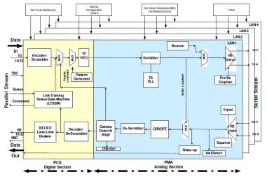
PCI Express Gen 1/2/3/4 Phy
- TSMC advanced 16 nm FFC CMOS process
- Available in 1X, 4X, 8X, and 16X configuration
-
PCI Express Gen 1/2/3/4 Phy
- 2.5/5.0/8/16 Gbps per lane interface optimized for PCI Express applications
- Compliance to PCI Express 1.0a, 1.1 and 2.1, 3.1 and 4.0 PIPE specifications
-
UltraScale+ Device Integrated Block for PCI Express (PCIe)
- Designed to PCI Express Base Specification 3.1
- PCI Express Endpoint, Legacy Endpoint or Root Port Port Modes
- x1, x2, x4, x8 or x16 link widths
- Gen1, Gen2 and Gen3 link speeds
-
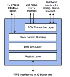
PCIe 3.1 Controller
- Dynamically adjustable application layer frequency down to 8Mhz for increased power savings
- Optional MSI/MSI-X register remapping to memory for reduced gate count when SR-IOV is implemented
- Configurable pipelining enables full speed operation on Intel and Xilinx FPGA, full support for production FPGA designs up to Gen3 x16 with same RTL code
- Ultra-low Transmit and Receive latency (excl. PHY)
- Smart buffer management on receive side (Rx Stream) and transmit side (merged Replay/Transmit buffer) enables lower memory footprint
-
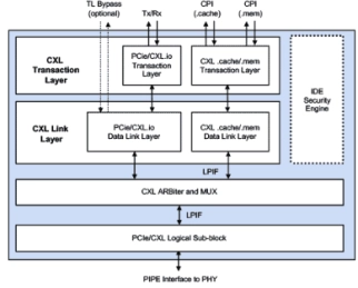
CXL 3.1 Controller
- Ultra-low Transmit and Receive latency
- Internal data path size automatically scales up or down (256, 512 or 1024 bits) based on max. link speed and width for optimal throughput
- Supports backwards compatibility to PCIe 6.1
- Optional MSI/MSI-X register remapping to memory for reduced gate count when SR-IOV is implemented
- Optional QuickBoot mode allows for up to 4x faster link training, cutting system-level simulation time by 20%
- Loopback Mode support at DLL for CXL.mem and CXL.cache protocols
- Merged Replay and Transmit buffer enables lower memory footprint
-
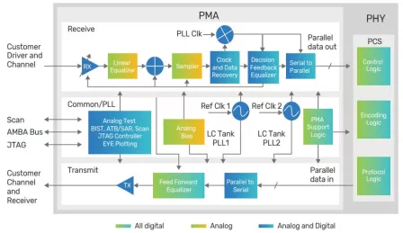
10Gbps Multi-Protocol PHY IP (+PCIe 3.1)
- Supports 10G-KR, PCIe 3.1/2.0/1.0, XAUI, Q/SGMII, and Gigabit Ethernet
- LC tank PLL with a wide range of reference clock frequencies and SSC
- High-performance decision feedback equalization and adaptive CTLE
- Serial and parallel loop-back functions
- Available in X1 through X10 lane configurations