Memory IP
Filter
Compare
3,192
IP
from
254
vendors
(1
-
10)
-
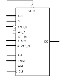
Single Port High-Speed Multi Bank SRAM Memory Compiler on GF 22FDX+
- Ultra-Low Leakage - GLOBALFOUNDRIES low-leakage 6T L110 bit cells with High Vt and low leakage periphery to ensure minimal leakage and high yield.
- Multi-Bank Architecture - Memory split into 1 to 4 banks for reduced bit line length and enhanced timing.
- Ultra Low Power Standby - Built-in source biasing trims standby current to a minimum for data retention.
-
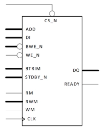
Single Port Low Leakage SRAM Memory Compiler on GF 22FDX+
- Ultra-Low Leakage: High VT (HVT) and low leakage (LLHVT) devices are used with source biasing to minimize standby currents while operating at low voltage
- Bit Cell: Utilizes GlobalFoundries® Ultra-Low Leakage, 6T(L110) bit cells to ensure high manufacturing yields
- Five Power Modes: High Performance, Low Leakage, Standby, Retention, and Power Off modes provide flexibility for power optimization

-
Single Port Low Leakage SRAM Memory Compiler on GF 22FDX+
- Ultra-Low Leakage: High VT (HVT) and low leakage (LLHVT) devices are used with source biasing to minimize standby currents while operating at low voltage
- Bit Cell: Utilizes GlobalFoundries® Ultra-Low Leakage 6T (P110UL) bit cells to ensure high manufacturing yields
- Five Power Modes: High Performance, Low Leakage, Standby, Retention, and Power Off modes provide flexibility for power optimization
- Speed Grades: Three options to adjust the speed/leakage balance and optimize for high speed or low power operation
-
Functional-Safety & Secure LPDDR3 Memory Subsystem
- Safe & Secure-LPDDR3 that is ready for ASIL (Automotive Safety Integrity Level) and secure by design
- Functional Safety out-of-the box design, with an extensive ASIL documentation package.
- Integrated security features into the controller. Characterized for extended operating conditions and long-term reliability.
-
Hyper-Bandwidth Multichannel Memory Subsystem
- Hyper-Bandwidth Multi-Channel - The fastest, most observable LPDDR3 subsystem you can drop into an SoC
- Supports an aggressive bandwidth envelope for LPDDR3, JEDEC-2133Mbps and up to 3200 Mbps on select process nodes.
- Includes hard QoS enforcement, traffic shaping, performance observability & self-tuning PHY front-end.
-
sROMet compiler - Memory optimized for high density and low power - Dual Voltage - compiler range up to 1M
- Foundry sponsored - sROMet compiler - TSMC 55 nm uLPeFlash - Non volatile memory optimized for high density and low power - Dual Voltage - compiler range up to 1M
-
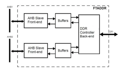
Fault Tolerant DDR2/DDR3/DDR4 Memory controller
- FTADDR is a memory controller for DDR2,DDR3 and DDR4 SDRAM memory devices.
- It uses a strong error correction code to achieve exceptional fault tolerance
-
Memory Compilers
- Dolphin provides a wide range of Memory Compilers and Specialty Memory (ROM, Multi Port RF, CAM, etc.) optimized to meet even the most demanding requirements for high performance, high density and low power.
-
DDR4 IO for memory PHY, 3200Mbps on SMIC 40nm
- The DDR4 IO is used to transfer the Command/Address/Clk and Data between the memory controller PHY and the DRAM device
- The TX is designed to send information from PHY to DRAM and RX is designed to receive information which is from DRAM.
-
PHY IO for PSRAM memory PHY, 1066Mbps on TSMC 22nm
- The PHYIOs is used to transfer the Command/Address/Clk and Data between the memory controller PHY and the PSRAM device
- The TX is designed to send information from PHY to PSRAM and RX is designed to receive information which is from PSRAM
- there are bi-direction DQ IO, TX-only CK IO, filler cell with differrent size and VDDQ/VSS power clamp IO included in the PHYIOs.