Legacy-Compatible 8051 IP
Filter
Compare
5
IP
from
3
vendors
(1
-
5)
-
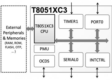
Ultra-Small 8051-Compatible Microcontroller
- The T8051XC3 core implements one of the smallest-available 8-bit MCS®51-compatible microcontrollers.
- The core integrates an 8051 CPU with a serial communication controller, flexible timer/counter, multi-purpose I/O port, interrupt controller, and optionally with a debug unit supporting JTAG and Single-Wire interfaces.
-
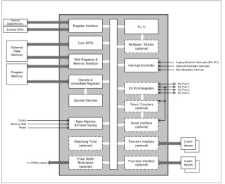
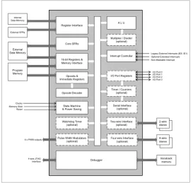
Legacy-Configurable 8051-Compatible Microcontroller IP
- Fully compatible with the MCS® 51 instruction set
- Configurable CPU architecture: 12, 6, or 4 clock cycles per machine cycle
- Extensive set of optional features and peripherals
- JTAG-based On-Chip Debug Support (OCDS)
-
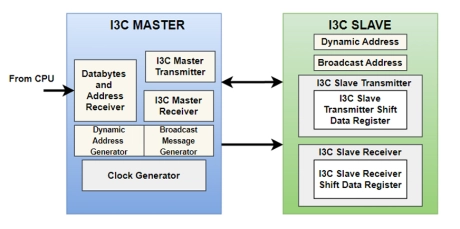
I3C - Function Controller
- The I3c protocol, short for " Improved Inter - Integrated Circuit," is a communication protocol designed to improve upon the widely - used I2C protocol.
- It was developed by the MIPI Alliance, a global organization that aims to develop interface specifications for mobile devices.
-
M8051EW V3.0+ Fast 8-bit Microcontroller with on-chip debug
- Binary and Memory cycle compatible with the Intel 8051•
- Optional conditional branch acceleration
- Up to eight 16-bit data pointers
- 25-input, five level interrupt controller
-
M8051W V 5.0 Fast 8-bit Microcontroller
- Binary and Memory cycle compatible with Intel 8051 Designs
- Fast 2-clocks per machine cycle implementation
- 1Mbyte program and data address spaces
- Memory interfaces may be configured for synchronous or asynchronous devices