DFT IP
Filter
Compare
50
IP
from
20
vendors
(1
-
10)
-
Discrete Fourier Transform (DFT)
- A fixed point bit-accurate C-Model to enable system level analysis of Xilinx DFT core.
- Transform sizes from 12 to 1200 points with the option to change size frame by frame.
- Less than 26 us total latency when transforming 1200 points at 245.76 MHz (using any combination of sizes)
- Up to 18-bit two’s complement input data width, up to 18-bit two’s complement output data width with 4-bit block exponent.
-
Non-Power-of-Two FFT
- Sample Rates: Very high clock speeds
- FFT size: any size set of transforms (chosen at run-time) factorable into bases up to ~10
-
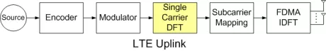
LTE Single Carrier FFT Circuit
- High Throughput: obtained from high clock rates (>400MHz using 65nm technology) and novel algorithms
-
HBM4 PHY IP
- Supports JEDEC HBM4 DRAMs
- Supports data rates up to 12 Gbps
- Supports up to 32 independent 64-bit memory channels
- Pseudo-channel operation supported to enable up to 64 32-bit pseudo-channels with 2048-bit PHY
-
Integer-N PLL, 32M ~ 256MHz on UMC 55nm
- This present IP is a Phase Locked Loop (PLL) circuit
- It’s analog PLL suitable for various frequency node generations
- The VCO can run from 32MHz to 256MHz
- It contains input clock divider (DIVM), a feedback clock divider (DIVN) and level shifter block to switch signals between VDD12 and VDD33
-
FFT Algorithm Accelerator
- Support transform point sizes n = 2^m, m = 4 ~ 12
- Support 16-bit and 32-bit fixed-point data formats
- Support bus max transmission width 64bit
- Support Radix-2 Decimation-In-Time (DIT) and Decimation-In-Frequency (DIF) FFT, IFFT algorithms
-
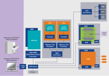
SLM SHS IP
- The SLM SHS IP is an automated hierarchical test solution for efficiently testing SoCs or designs using multiple IP/cores, including analog/mixed-signal IP, digital logic cores and interface IP.
- It significantly reduces test integration time by automatically creating a hierarchical IEEE 1500 network to access and control all IP/cores at the SoC level, and increases test quality of results (QoR), including optimizing test time and power through flexible test scheduling of IP and cores.
-
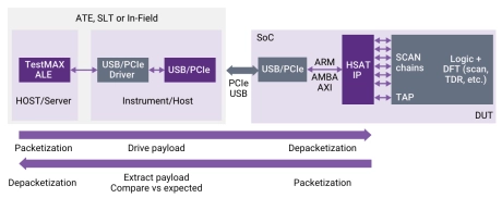
SLM High-Speed Access & Test IP
- The SLM High-Speed Access and Test (HSAT) IP combined with the TestMAX® ALE software uses standard high speed IO interfaces such as PCIe and USB, to get test, debug and monitoring data in and out of an SoC at Gigabit data rates and avoids the need for large numbers of test and interface pins.
- Test time can be reduced because the link between the test time and GPIO data rate is eliminated. Further, this solution provides a key component for Synopsys Silicon Lifecycle Management solution allowing manufacturing tests to be repeated in-system and in-field as well as providing high speed access to PVT and functional monitor dat
-
MRDIMM DDR5 & DDR5/4 PHY & Controller
- The DDR IP Mixed-Signal MRDIMM DDR5 PHY and DDR5/4 Combo PHY provide turnkey physical interface solutions for ICs requiring access to JEDEC compatible SDRAM or MRDIMM/ RDIMM/ LRDIMM/ UDIMM DDR5 devices
- It is optimized for low-power and high-speed applications with robust timing and small silicon area
- It supports all JEDEC DDR5/4 SDRAM components in the market
-
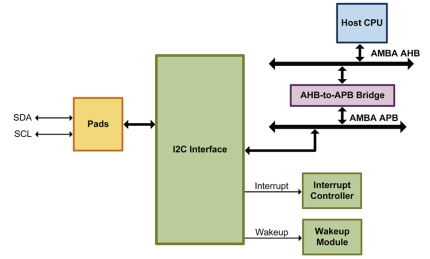
APB I2C Master/Slave Controller
- The I2C Interface provides full support for the two-wire I2C synchronous serial interface, compatible with the ACCESS.
- Bus physical layer, with additional support for the SMBus protocol, including Packet Error Checking (PEC).
- Through its I2C compatibility, it provides a simple interface to a wide range of low-cost memories and I/O devices, including: EEPROMs, SRAMs, timers, A/D converters, D/A converters, clock chips, and peripheral drivers.