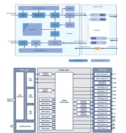
Controller IP
Filter
Compare
3,444
IP
from
198
vendors
(1
-
10)
-
JESD204E Controller IP
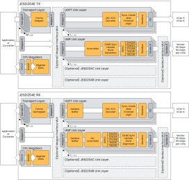
- The JESD204E Controller IP from Chip Interfaces is an early adopter’s version of the upcoming revision of the JEDEC standard for Serial Interface for Data Converters.
- The JESD204-E IP core supports the UCIe Optimized Link Layer, a dedicated mode to run JESD over UCIe Modules with Line rates up the 64Gbps per bump, and a JESD204D backwards compatible mode called the Unified Link Layer with line speeds up to 116Gbps with PAM4 and 58Gbps with NRZ and full FEC support.
-
UALink Controller
- The UALink Controller, part of Cadence’s verified UALink IP subsystem, delivers ultra-low latency and high-bandwidth interconnects that enable seamless scale-up connectivity between AI accelerators. I
- t supports memory semantics for read, write, and atomic operations, ensuring fast, coherent data handling across workloads. UALink IP provides a scalable, future-ready solution for next-generation AI infrastructure.
-
eFuse Controller IP
- AMBA 3.0 APB interface for register access
- Automated eFuse read, program, and reload operations
- Protection against repeated programming of the same bits
- Support for 32-bit aligned read/program operations
-
HBM4 Controller IP
- Supports JEDEC standard HB4 DRAM
- DFI 5.1 compliant interface to HBM4 PHY
- Multiport Arm® AMBA® interface (AXI™) with managed QoS per pseudo-channel or single-port host interface(HIF), per channel
-
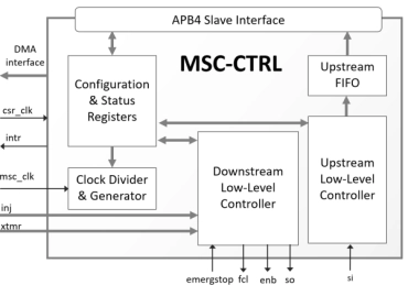
Microsecond Channel (MSC/MSC-Plus) Controller
- The MSC-CTRL IP core implements a high-speed serial interface controller designed to connect a microcontroller or SoC to external power devices or sensors.
- It implements the Microsecond Channel (MSC) and Microsecond Channel Plus (MSC-Plus) protocols—derived from the Microsecond Bus (uSB) serial concept—and acts as a bus master for downstream transmission and as a bus slave for upstream transmission.
-
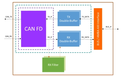
CAN-FD Controller
- The Controller Area Network (CAN) is a highly reliable serial bus protocol defined in the Bosch CAN specifications for standard CAN 2.0B and CAN FD, as well as ISO 11898-1:2024.
- The TES CAN Flexible Data-Rate Controller IP core is a Hardware IP core written in VHDL.
-
LPDDR6/5X/5 Controller IP
- Supports JEDEC standard LPDDR6, LPDDR5X and LPDDR5 SDRAMs
- Support for data rates up to 14.4 Gbps for LPDDR6, 10.67 Gbps for LPDDR5X, and 6.4 Gbps for LPDDR5
- Multiport Arm® AMBA® interface AXI™4 with managed QoS or single-port host interface to the DDR controller
- DFI 5.2 compliant interface to Synopsys LPDDR6/5X/5 PHY

-
PCIe PHY and controller solution
- Brite 16Gbps PCIe PHY and controller solution provide high efficient interconnection that is optimized for PPA performance. The System can support short-reach or long-reach channels for plenty application scenarios.
- Brite PCIe controller to AXI architecture provides a high-performance, easy-to-use interconnect solution between PCI Express and the latest version of the AXI protocol. It inherits the leading architecture and features an AXI user interface with built-in DMA, compliant with the AMBA® AXI3 and AXI4 specifications.
-
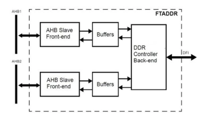
Fault Tolerant DDR2/DDR3/DDR4 Memory controller
- FTADDR is a memory controller for DDR2,DDR3 and DDR4 SDRAM memory devices.
- It uses a strong error correction code to achieve exceptional fault tolerance
-
PCIe Controller
- Dolphin PCIe Controller is a high-performance and compact solution for PCIe provide high-throughput, low-latency, and power-efficient external connectivity in SoCs for mobile, networking, storage, cloud computing, and automotive applications.
- The PCIe Controller consists of silicon-proven digital controllers, PHYs and verification IP, all of which are designed to support all required features of the PCIe 5.0 32GT/s (Gen5), PCIe 4.0 16GT/s (Gen4), 3.1 8GT/s (Gen3), 2.1 5GT/s (Gen2) and 1.1 2.5GT/s (Gen1).