Interface IP Cores for TSMC
Welcome to the ultimate
Interface IP Cores
for
TSMC
hub! Explore our vast directory of
Interface IP Cores
for
TSMC
All offers in
Interface IP Cores
for
TSMC
Filter
Compare
699
Interface IP Cores
for
TSMC
from
34
vendors
(1
-
10)
-
Ultra-Low Latency 32Gbps SerDes IP in TSMC 12nm FFC
- Modular architecture supporting x1 to x16 lanes with a single CMU
- Lane-based PLL architecture supporting flexible, independent data rates from 1.25 to 32Gbps
- Ultra-low latency 2/4/8-bit parallel interface mode for lowest possible latency
-
Ultra-Low Latency 32Gbps SerDes IP in TSMC 22nm ULP
- Modular architecture supporting x1 to x16 lanes with a single CMU
- Lane-based PLL architecture supporting flexible, independent data rates from 1.25 to 32Gbps
- Ultra-low latency 2/4/8-bit parallel interface mode for lowest possible latency

-
32Gbps SerDes IP in TSMC 12nm FFC
- Modular architecture supporting x1 to x16 lanes with a single CMU
- Lane-based PLL architecture supporting flexible, independent data rates from 1.25 to 32Gbps
- Configurable low latency parallel data interface for optimal system performance
-
32Gbps SerDes IP in TSMC 22nm ULP
- Modular architecture supporting x1 to x16 lanes with a single CMU
- Lane-based PLL architecture supporting flexible, independent data rates from 1.25 to 32Gbps
- Configurable low latency parallel data interface for optimal system performance
-
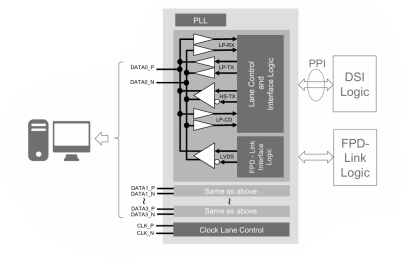
MIPI D-PHY and FPD-Link (LVDS) Combinational Transmitter for TSMC 22nm ULP
- Technology is TSMC 22nm ULP 1p10M.
- Supply voltage can be applied 1.0V for core voltage, 1.8V for IO voltage.
- Maximum data rate of each channel is 1.5Gbps at High-speed mode for MIPI D-PHY Transmitter.
- Data rate of each channel is 609Mbps for FPD-Link(LVDS).
-
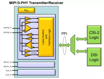
MIPI D-PHY Transmitter/Receiver for TSMC 40nm LP
- Renesas MIPI D-PHY Transmitter/Receiver can be used for analog Transmitter/Receiver of following interface.
- Technology is TSMC 40nm LP 1p6M (4x1z) .
- Supply voltage can be applied 1.1V for core voltage, 1.8V for IO voltage.
-
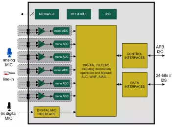
24-bit Cap-less ADC 106 dB SNR with ASRC 6 channels
- I2C and APB control interface
- Embedded low noise voltage regulator for best resilience to power supply noise
- Low BoM and capacitor-less input connection
- High dynamic range for high quality recording in far-field applications
-
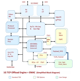
1G TCP Offload Engine TOE Very Low Latency (TOE)
- Ideal for high performance and mid performance specialized, differentiable ASICs or FPGAs for Network security or Network infrastructure applications
- Less than 4000 Xilinx slices, Altera ALMs or 150,000 ASIC gates + on-chip memory
- Fully integrated 100 M bit/1-G bit high performance EMAC.
- Scalable MAC Rx FIFOs and Tx FIFOs make it ideal for optimizing system performance.
-
24-bit -130dB THD+N Multi-Channel Audio Sample Rate Converter
- This core can be used to interface digital audio equipments operating at different sample rates.
- It has been designed for systems requiring very high quality in terms of low harmonic distortion and noise, tolerance and rejection of input jitter.
-
16-bit -90dB THD+N Multi-Channel Audio Sample Rate Converter
- This core can be used to interface digital audio equipments operating at different sample rates.
- It has been designed for systems that require a low-cost solution, maintaining low harmonic distortion and noise, and a high tolerance and rejection of input jitter.