TSMC CLN12FFCP 12nm LPDDR3 PHY - 2133Mbps
Overview
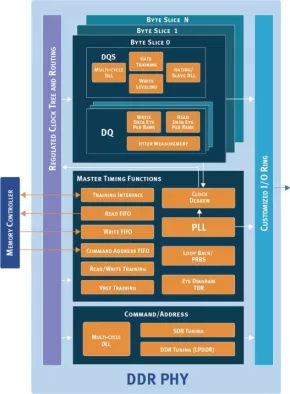
The TCI LPDDR PHY is a high-performance, scalable system using a radically new architecture that continuously and automatically adjusts each pin individually, correcting skew within byte lanes. This state-of-the-art tuning acts independently on each pin, data phase and chip select value. Read gate and data eye timing are also continuously adjusted. Automatic training is included for multi-cycle write leveling and read gate timing, read/write data eye timing, and PHY Vref and DRAM Vref settings. Remarkable physical flexibility allows the PHY to adapt to each customer’s die floorplan and package constraints, yet is delivered and verified as a single unit for easy timing closure with no assembly required. The PHY is DFI 5.1 compliant, and when combined with an appropriate LPDDR memory controller, a complete and fully-automatic LPDDR system is realized.
Key Features
- Supports LPDDR3
- DFI 5.1 compliant
- Supports x4, x8 and x16 DRAMs
- Up to 72 bits wide and up to 4 ranks
- Includes PLL, with frequency multiplication from low frequency reference
- Per pin architecture automatically corrects skew, increases data eye and eliminates most parallel interface problems
- Fully automatic training is managed by a light weight special purpose processor
- Continuous adjustment of read gate and data eye timing
- Localized and optimized PHY-to-memory controller interface to ease timing closure
- Full speed read/write BIST with pseudo-random data, mux-scan ATPG and 1149.1 Boundary Scan
Benefits
- Automatic Deskew - Skew among pins is automatically corrected; intentional skew can reduce SSO
- Tuning - State-of-the-art tuning is the key to a high performance DDR system
- Complete PHY - Completely assembled and validated hard PHY and I/O ring means no assembly is required and performance is guaranteed
- Compatible - DFI 5.1 compliance and PHY independent training allows for compatibility with a variety of memory controllers
- Flexibility - Proprietary tools generate and validate a PHY fitted to the customer’s die floorplan and package
- Timing Closure - Memory controller to PHY timing closure is simplified by a localized synchronous interface
- Instrumentation - PHY resources can measure data eye and jitter per pin, speeding up board bring-up
Block Diagram

Deliverables
- GDSII and LVS Spice netlist, behavioral, synthesis and LEF models for hard macros
- RTL code and SDC constraints for soft logic
- IBIS and Spice models for RDL, package and PCB simulations
- Extensive user documentation
- Integration support to ensure a successful tapeout
Technical Specifications
Short description
TSMC CLN12FFCP 12nm LPDDR3 PHY - 2133Mbps
Vendor
Vendor Name
Foundry, Node
TSMC LPCLN12FFC+
Availability
Yes
TSMC
Pre-Silicon:
12nm