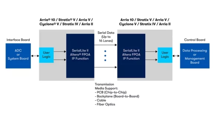
The Serial Lite II Intel® FPGA IP core provides a simple and lightweight way to move data from one point to another reliably at high speeds. It consists of a serial link of up to 16 bonded lanes with logic to provide a number of basic and optional link support functions. The Atlantic* interface is the primary access for delivering and receiving data.
The Serial Lite II protocol specifies a link that is simple to build, uses as little logic as possible, and requires little work to implement. The Serial Lite II Intel® FPGA IP is feature-rich, and can be parameterized through a powerful graphical user interface (GUI).
A link built using the Serial Lite II Intel® FPGA IP core can operate from 622 Mbps to 6.375 Gbps per lane. Intel® Arria® 10 devices that are using the IP core can operate well above 6.375 Gbps per lane. The 8B/10B encoding scheme and optional cyclic redundancy check (CRC) capabilities enhances link reliability. Further reductions in the bit error rate can be achieved using the optional retry-on-error feature. Data rate and consumption mismatches can be accommodated using the optional flow-control feature to ensure that no data is lost.
Note that the Intel® Arria® 10 and Cyclone® V device families indirectly support the use of the Serial Lite II Intel® FPGA IP core in the Intel® Quartus® Prime software. If your design requires the IP core on Intel Arria® 10 or Cyclone® V devices, please contact your local sales representative for a special license and easy-to-follow implementation guidelines.