Perceptia’s DeepSub™ pPLL03F is an all digital PLL featuring low-jitter and compact area suitable for clocking applications with critical timing requirements at frequencies up to 4GHz. It is suitable as a clock source for performance computing blocks and ADCs/DACs with moderate SNR requirements.
To give SoC designers the maximum flexibility in building complex multi-domain clock systems, pPLL03F is very small (< 0.004 sq mm) and low power (< 1.3 mW). It is well suited to applications with many clock domains where each is driven by their own PLL. To simplify system design, PLL03 has an integrated power supply regulator which allows multiple instances of PLL03 to share common power supplies. Alternatively instances of pPLL03 can share supplies with the blocks that use its output clock.
pPLL03 integrates easily into any SoC design and includes all the views and models required by modern back end flows.
The pPLL03F is built using Perceptia’s second generation all digital PLL technology. This robust technology delivers identical performance regardless of PVT conditions. It consumes a small fraction of the area of an analog PLL whilst maintaining comparable performance.
pPLL03F can be used as an integer-N PLL or as a fractional-N PLL. The fractional-N mode provides a high flexibility to choose the best combination of input and output clock frequencies at the system level.
Perceptia further provides integration support and offers customization and migration services.
Fractional-N PLL for Performance Computing in Samsung 14LPP
Overview
Key Features
- Low jitter, suitable for many clocking applications, including high speed digital, ADC, DAC, medium-speed PHY
- Extremely small die area (< 0.004 sq mm), using a ring oscillator
- Output frequency can be from 1 to 400 times the input reference, up to 4GHz
- Reference clock from 10MHz to 500MHz
- Second-generation digital PLL architecture, providing integer and fractional multiplication
- Two PLL outputs via separate postscalers
- Post-scalers programmable from 1 to 2,040
- Lock-detect output
- Can generate a spread-spectrum clock from a clean reference
- Oscillator output duty cycle better than 48 / 52% on CK_PLL_OUT0 and CK_PLL_OUT1
- Highly testable using industry standard flows
- ATPG vectors provided
- Specification of functional tests to supplement ATPG testing
- Industrial operating conditions (-40 to 85°C) with junction temperature up to 100°C
Benefits
- Fractional multiplication with frequency up to 4GHz
- Low jitter (< 10 ps RMS)
- Small size (< 0.004 sq mm)
- Low Power (< 1.3 mW)
- Support for multi-PLL systems with tens of PLLs per SoC
- Easy integration
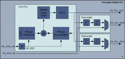
Block Diagram
Applications
- Performance Computing
- Complex SoCs with many clock domains
- Low-jitter applications
- Moderate SNR ADC/DAC
Deliverables
- Datasheet
- Detailed Verilog behavioral model
- Timing models
- LEF5.6 abstract for floor planning/chip assembly
- Integration Guide
- DFT Guide
- Integration support
- Characterization report
- GDSII layout macrocell
- CDL netlist for LVS
- DRC, LVS and SI verification reports
- Netlist model with accompanying documentation allowing integration of the module in scan chains
Technical Specifications
Short description
Fractional-N PLL for Performance Computing in Samsung 14LPP
Vendor
Vendor Name
Foundry, Node
Samsung 14LPP. Portable to all CMOS processes 65nm and smaller.
Maturity
In development
Availability
Q1 2021
Samsung
Pre-Silicon:
14nm
Related IPs
- Wide Range Programmable Integer PLL on Samsung 14LPP
- 40nm 1.1V 2GHz-4.7GHz Fractional-N RF Quadrature PLL
- 40nm 1.1V 6.0GHz-9.4GHz Fractional-N RF PLL
- 12-bit, 2 GSPS High Performance ADC in 16nm CMOS
- 12-bit, 6 GSPS High Performance RF ADC in 16nm CMOS
- 12-bit, 7 GSPS High Performance RF DAC in 16nm CMOS