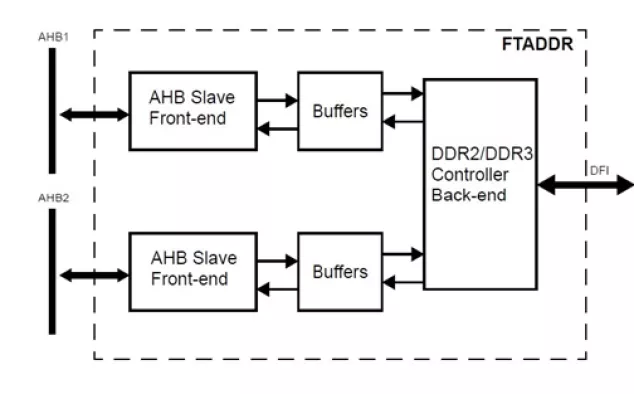
FTADDR is a memory controller for DDR2 and DDR3 SDRAM memory devices. It uses a strong error correction code to achieve exceptional fault tolerance.
On the memory side, it presents a DFI interface for connection to an on-chip physical layer (PHY) that manages the low-level timing and data recovery and then provides the I/O buffers. Towards the system-on-chip, it presents the memory through an AMBA AHB slave interface.
DDR2 & DDR3 Fault Tolerant Memory Controller
Overview
Key Features
- Configurable to have multiple AHB ports with concurrent accesses to different memory banks
- 96-, 64- or 32-bits interface towards SDRAM
- Memory devices of width x8 or x4
- Support for several PHYs:
- Generic DFI
- Altera UniPhy (64 bits)
- Xilinx Ultrascale (64 or 64+32)
- Strong error correction code to achieve double device correction capability:
- Deliver correct data despite one full device failure and random SEU-induced errors on the other devices.
- Up to 8 parallel banks (chip selects)
- Can operate autonomously:
- Designed to support also processor-less configurations
Block Diagram

Deliverables
- FTADDR can be synthesized with common commercial synthesis tools.
- The IP model is highly configurable and portable between different implementation technologies, for both FPGA and ASIC. For ASIC implementations, a DFI compliant PHY and SSTL IO buffers are also required
- FTADDR is available as a separate package or as an addition to commercial versions of the GRLIB VHDL library.
- Example designs for Xilinx and Altera FPGA evaluation boards are readily available.
Technical Specifications
Related IPs
- xSPI Multiple Bus Memory Controller
- Quad SPI Flash Memory Controller
- Universal Multi-port Memory Controller for RLDRAM2/3, DDR5/4/3, DDR4 3DS and LPDDR3/2 and LPDDR3/2
- Universal Multi-port Memory Controller for RLDRAM2/3, DDR4/3, DDR4 3DS and LPDDR3/2 and LPDDR3/2
- Hyperbus Flash Memory Controller
- HBM2/2E Memory Controller Core