Samsung Foundry 14LPP IP
Filter
Compare
2
IP
from
2
vendors
(1
-
2)
-
32G PHY, Samsung 10LPP x4, North/South (vertical) poly orientation
- Supports 1.25 to 32 Gbps data-rate
- Supports PCI Express 5.0, 1G to 400G Ethernet, CCIX, CXL, and SATA protocols
- Supports x1 to x16 macro configurations with aggregation and bifurcation
- Spread Spectrum Clock (SSC)
-
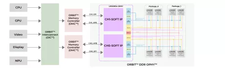
LPDDR5/4x/4 PHY IP for Samsung 14LPU
- Compliant with JEDEC standards for LPDDR5/4x/4 with PHY standards
- DFI 5.0 Interface Compliant
- Supports 1,2, or 4 ranks
- Multiple frequency states