DRAM memory controller IP
Filter
Compare
353
IP
from
30
vendors
(1
-
10)
-
DDR5 & DDR4 COMBO IO for memory controller PHY, 4800Mbps on TSMC 12nm
- The DDR5&DDR4 COMBO IO is used to transfer the Command/Address/Clk and Data between the memory controller PHY and the DRAM device
- The TX is designed to send information from PHY to DRAM and RX is designed to receive information which is from DRAM._x000D_ It supports DDR5&DDR4 interface
- The DDR5 DQ data rate can be up to 4800Mb/s, and the DDR4 DQ data rate can be up to 3200Mb/s and CA is SDR mode.
-
DDR4 & LPDDR4 COMBO IO for memory controller PHY, 3200Mbps on TSMC 22nm
- The DDR4&LPDDR4 COMBO IO is used to transfer the Command/Address/Clk and Data between the memory controller PHY and the DRAM device
- The TX is designed to send information from PHY to DRAM and RX is designed to receive information which is from DRAM.
-
General Memory Controller
- The GMC (General Memory Controller) includes two memory controllers: The NOR/PSRAM memory controller, The Synchronous DRAM (SDRAM/Mobile LPSDR SDRAM) controller
-
High-Performance Memory Controller II SDRAM Intel® FPGA IP Core
- The High-Performance Memory Controller II SDRAM Intel FPGA IP core handles the complex aspects of using DDR, DDR2, and DDR3 SDRAM at speeds up to 933 MHz
- The intellectual property (IP) core initializes the memory devices, manages SDRAM banks, translates read-and-write requests from the local interface into all the necessary SDRAM command signals, and performs command and data reordering.

-
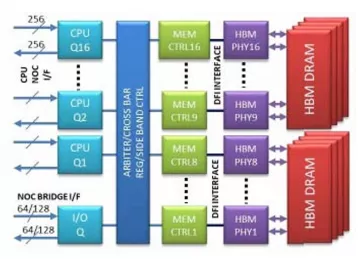
HBM Memory Controller
- Low latency, high bandwidth
- Supports HBM or DDRx memory types
- 16 parallel access channels
- Multi, independent internal queues
-
DDR3 SDRAM Memory Controller
- Supports DDR3 SDRAM memory devices on AMD-Xilinx 7 Series FPGAs
- Size optimized – ideal for low cost 7 Series FPGAs (Artix-7, Spartan-7)
-
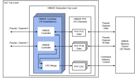
HBM3 Memory Controller
- High Bandwidth Memory (HBM) DRAM controller
- Supports AXI 4.0 port
- Supports DFI1: 2
- Supports BL8
-
HBM3E/3 Memory Controller
- Supports HBM3E / HBM3 memory devices
- Supports all standard HBM3 channel densities (up to 32 Gb)
- Supports up to 9.6 Gbps/pin (HBM3E) or 8.4 Gbps/pin (HBM3)
- Refresh Management (RFM) support
- Maximizes memory bandwidth and minimizes latency via Look-Ahead command processing
- Integrated Reorder functionality
-
High Performance DDR 3/2 Memory Controller IP
- Supports DDR3/DDR2 SDRAM
- 16 bits width DDR2/DDR3 SDRAM Interface
- Memory Clock up to 462MHz, DFI Clock up to 462MHz
- Support DDR2 667/800/1066 and DDR3 667/800/1066/1333/1600/1866
-
LPDDR3/4 Memory Controller IP
- a. DDR3-LPDDR3 and DDR4-LPDDR4 modes up to 2133Mbps, and 2800Mbps,respectively
- b. x16/x32 data path interface extendable
- c. JEDEC 1.2V SSTL I/Os and 1.1V LVSTL I/Os
- d. Multiple drive strengths adjustable