DDR3-2133/LPDDR2 Combo IP
Filter
Compare
294
IP
from
44
vendors
(1
-
10)
-
DDR5 & DDR4 COMBO IO for memory controller PHY, 4800Mbps on TSMC 12nm
- The DDR5&DDR4 COMBO IO is used to transfer the Command/Address/Clk and Data between the memory controller PHY and the DRAM device
- The TX is designed to send information from PHY to DRAM and RX is designed to receive information which is from DRAM._x000D_ It supports DDR5&DDR4 interface
- The DDR5 DQ data rate can be up to 4800Mb/s, and the DDR4 DQ data rate can be up to 3200Mb/s and CA is SDR mode.
-
DDR4 & LPDDR4 COMBO IO for memory controller PHY, 3200Mbps on TSMC 22nm
- The DDR4&LPDDR4 COMBO IO is used to transfer the Command/Address/Clk and Data between the memory controller PHY and the DRAM device
- The TX is designed to send information from PHY to DRAM and RX is designed to receive information which is from DRAM.
-
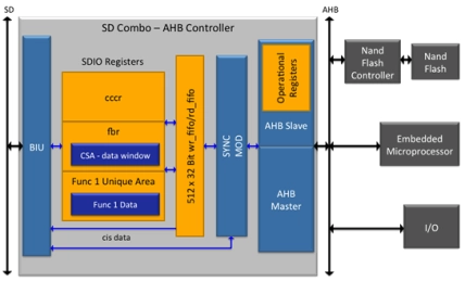
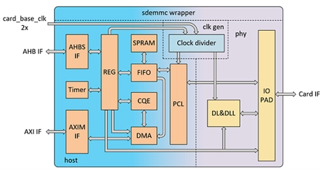
SD Card / SDIO Card Combo Device IP
- SD / SDIO Card Combo Device IP core is SD memory controller and a SDIO controller with an AHB interface.
- Combining with the optional NAND Flash Controller IP, the SD/SDIO Combo Device IP provides an integrated SD memory Card solution for designs that utilize NAND flash memory.
-
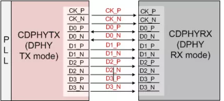
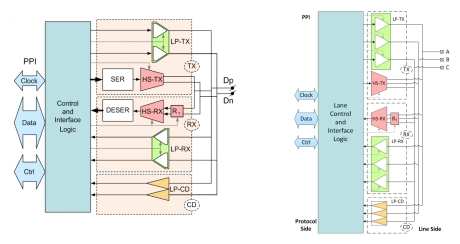
MIPI C-PHY℠ v2.0 + D-PHY℠ v2.5 Combo IP Core
- This Tx/Rx transceiver complies with the MIPI Alliance C-PHY℠ v2.0 and D-PHY℠ v2.5 specifications, with world-class area and power dissipation, and is available for a range of foundry processes.
- This IP delivers 6 Gbps per lane for a max throughput of 24 Gbps in D-PHY℠ mode, and 6 Gsps per trio for a max throughput of 41.04 Gbps in C-PHY℠ mode.
-
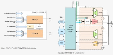
MIPI D-PHY/LVDS Combo Transmitter IP
- The MXL-LVDS-DPHY-DSI-TX is a combo PHY that consists of a high-frequency low-power, low-cost, source-synchronous, Physical Layer supporting the MIPI® Alliance Standard for D-PHY and a high performance 4-channel LVDS Serializer implemented using digital CMOS technology.
- In LVDS mode, both the serial and parallel data are organized into 4 channels. The parallel data is 7 bits wide per channel. The input clock is 25MHz to 150MHz. The serializer is highly integrated and requires no external components. The circuit is designed in a modular fashion and desensitized to process variations. This facilitates process migration, and results in a robust design.
-
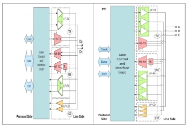
MIPI C-PHY/D-PHY Combo IP
- The MIPI C/D-PHY combo IP is a high-frequency low-power, low cost, physical layer compliant with the MIPI® Alliance Standard for C-PHY and D-PHY.
- The PHY can be configured as a MIPI Master or MIPI Slave, supporting camera interface CSI-2 v1.2 or display interface DSI v1.3 applications in the D-PHY mode. It also supports camera interface CSI-2 v1.3 and display interface DSI-2 v1.0 applications in the C-PHY mode.
-
eMMC/SD/SDIO Combo IP
- The eMMC/SD/SDIO Combo IP is a comprehensive solution designed to support high-performance storage and I/O connectivity for a wide range of applications
- This IP integrates a host controller and PHY, enabling seamless communication with eMMC, SD, and SDIO devices
- When connecting the SD/SDIO device, the IP supports DS, HS, SDR12, SDR25, SDR50, SDR104, and DDR50 speed modes
-
MIPI C/D Combo TX PHY and DSI controller
- High Data Rates: Supports data transmission rates
- Energy Efficiency: Optimized for low power consumption, making it ideal for battery-powered devices
- Complete Solution: Combines the MIPI CD-PHY Transmitter PHY and DSI Controller to make it a one-stop solution
- Flexible IP Configuration
-
DDR and LPDDR Combo PHY
- Supports multiple combinations of DDR/LPDDR interfaces
- Compliant with JEDEC DDR and LPDDR standards
- Supports all auto calibrations
- Industry leading area and power
-
MIPI C/D Combo PHY RX - GlobalFoundries 22FDX
- Supports up to one clock lane and four data lanes for DPHY1.2
- Fully compliant with MIPI D-PHY v1.2 and C-PHY v1.0 spec
- Available in GlobalFoundries 22FDX process
- Three 3phase encoded data lanes for CPHY1.0