BCH ECC IP
Filter
Compare
15
IP
from
8
vendors
(1
-
10)
-
BCH ECC Core IP
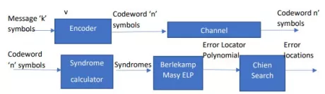
- The patent-pending Dynamically Configurable BCH technology is the base for the BCH ECC engine incorporating BCH coders and decoders configurable for a wide range of code-length for high performance and high data rate error corrections.
- The BCH ECC engine with configurable code-length BCH coders and decoders performs the Inversion-less Berlekamp-Massey Algorithm (IBMA) to generate or decode the ECC code on each clock.
-
ECC with BCH Algorithm
- High bandwidth, low latency parallel encode and decode paths
- Configurable number of encode blocks
- Configurable number of decode blocks
- Configurable code word length (K), up to 1024 bytes
-
BCH Error Correcting Code ECC
- Asynchronous operation
- No clocks required.
- No storage like memories SRAMS/ROMS/FilipFlops used
- No iterative Feedback in the pipeline
-
BCH Encoder/Decoder IP Core
- Full hardware implementationfor maximum performance, encoding, errordetectionand correct
- Balanced performance/gatecount
- All Galois fields covered
- ValidatedIP reducesTime-To-Market
-
1KB/ECC96 NAND Flash BCH Encoder/Decoder
- 2-96 bit error correction
- 2-1800 data bytes per block
- Low-latency, synchronous interface
- Optional asynchronous ECC mode for faster correction computations
-
512B/ECC16 Nand Flash BCH Encoder/Decoder
- 2-16 bit error correction
- 2-900 data bytes per block
- Low-latency, synchronous design
- Pipelined correction operation supports 3 concurrent corrections
-
1KB/ECC40 NAND Flash BCH Encoder/Decoder
- 2-40 bit error correction
- 2-1800 data bytes per block
- Low-latency, synchronous design
- Pipelined correction operation supports 3 concurrent corrections
-
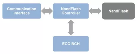
NAND Flash Controller
- Supports single-level and multi-level cells (SLC and MLC) NAND Flash devices.
- Supports 1, 4 and 8 bit ECC correction per 512byte.
- Uses Hamming code for SLC and BCH code for multi-bit correction in MLC.
- Programmable support for large block and small block NAND Flash devices with 512, 2k and 4k byte page sizes.
-
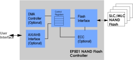
ONFI 4.2 NAND Flash Software Driver
- The NAND Flash Controller IP Core is a full-featured, easy to use, synthesizable core, easily integrated into any SoC or FPGA development. Designed to support SLC, MLC and TLC flash memories, it is flexible in use and easy in implementation.
- The controller works with any suitable NAND Flash memory device up to 1024Gb from leading memory providers – Micron, Samsung, Toshiba and Hynix.

-
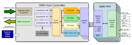
ONFI 4.2 NAND Flash Controller & PHY IP Compliant to JEDEC
- The NAND Flash Controller IP Core is a full-featured, easy to use, synthesizable core, easily integrated into any SoC or FPGA development.
- Designed to support SLC, MLC and TLC flash memories, it is flexible in use and easy in implementation. The controller works with any suitable NAND Flash memory device up to 1024Gb from leading memory providers – Micron, Samsung, Toshiba and Hynix.