Alphawave IP IP
Filter
Compare
10,118
IP
from
397
vendors
(1
-
10)
-
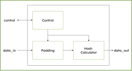
SHA-256 Secure Hash Algorithm IP Core
- Supports SHA-256 cryptographic algorithm, an one-way hash function compliant to NIST’s FIPS 180-4 standard.
-
SHA-512/384 - Secure Hash Algorithm IP Core
- Supports SHA-384, SHA-512 and SHA512/256 cryptographic algorithm, an one-way hash function compliant to NIST’s FIPS 180-4 standard.

-
DeWarp IP
- Real-Time Geometric Distortion Correction
- Precise Lens Distortion Compensation
- Advanced Image DeWarping Capabilities
-
LunaNet AFS LDPC Encoder and Decoder IP Core
- Rate 1/2
- GNSS, AFS
- Subframe 2/3/4
- Low implementation loss

-
-
Universal Chiplet Interconnect Express PHY IP - GLOBALFOUNDRIES® 22FDX®
- Delivered as Hardmacro IP
- Implementation of the physical layer of the UCIe standard from Raw D2D Interface (RDI) to electrical interface of UCIe main band (MB) and sideband (SB)
- Includes TX and RX side
-
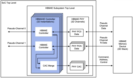
HBM4E Controller IP
- Supports HBM4/4E memory devices
- Supports all standard HBM4 channel densities (up to 32 Gb)
- Supports up to 16 Gbps/pin
- Refresh Management (RFM) support
-
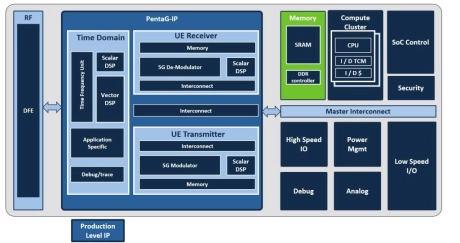
Third-Generation 5G-Advanced Modem IP Platform
- Ceva’s third-generation PentaG platform is a production-ready 5G-Advanced modem IP architecture that integrates baseband hardware, L1 PHY software, and comprehensive verification assets into a single reusable subsystem.
- Compared with the previous generation, the third-generation PentaG platform delivers substantial improvements in performance, scalability, and integration efficiency across both satellite and terrestrial deployments.
-
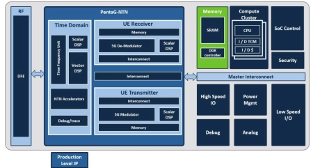
5G-NTN Modem IP for Satellite User Terminals
- Reduces integration complexity for satellite-focused design teams
- Accelerates time-to-silicon for 5G-NTN terminal SoCs
- Minimizes modem development risk with validated subsystem architecture
- Enables differentiation through programmable DSP and flexible software interfaces
-
5G-Advanced Modem IP for Edge and IoT Applications
- PentaG‑Edge is a fully integrated, plug‑and‑play 5G‑Advanced modem IP for IoT/industrial and terrestrial UE applications
- Multiple IoT use cases such as industrial 5G networks, robotics, drones, wearables, XR headsets, broadband CPE, V2X
- Enables rapid creation of custom modem products using an integrated modem solution aligned to 3GPP Rel‑18.
