Overview
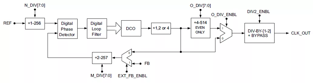
Granite SemiCom Inc. (GSC) has just completed the design, layout, and verification, of it’s digitall PLL (DPLL) for realization in TSMC’s 28nm HPM process; this is GSC’s third DPLL (developed over the previous five years). Fabrication is currently scheduled for the second quarter of 2014. The intended applications are for general purpose, moderately high speed, clock generation applications where small area and power are critical without sacrificing quality. Previous generations (realized in TSMC’s 40G and 40LP processes) were intended for the highest speeds possible for a PLL based on a wide-frequency-range ring-oscillator necessitating higher power. The new DPLL28 has traded off speed for greatly minimized power and area, yet retaining excellent jitter for the intended speeds (rms period jitter less than 0.1% of the ouput period). An example application might be for generating a clock in a DDR3 controller or in the CMU for multi-lane chip-to-chip serial links where a large number of CMUs are required.
Learn more about PLL IP core
How do you ensure that every part of a system receives the clock it needs—without wasting power or sacrificing performance? The answer lies in creating a well-structured frequency plan built around a PLL.
Jian Yang, Sween Kang (Synopsys)
This white paper is aimed at system architects and physical implementation leaders working on the design of SoCs. It can be confusing to understand the impact of different jitter sources and how to calculate a jitter budget when specifying a digital system. This white paper explains how jitter changes the period of a clock and how to ensure that jitter has correctly been accounted for in the calculations for timing closure.
This article explains a some of the key terminology and parameters commonly used to describe jitter. It will also help clarify the most important parameters for a some PLL applications, allowing the designer to better understand what is required from a PLL.
In high end RF systems, such as 5G radios, the requirements are so stringent that the source of this strongest unwanted tone can be the PLL. This article outlines how spurs in the input clock to the ADC or DAC may limit the SFDR. This in turn will set the requirements for the spurs for the input clock (from a PLL), in order to achieve a specific SFDR.
This article compares analog, first-generation digital, and second-generation digital PLLs. It evaluates which type of PLL may be best in which situation. It further discloses a roadmap into other application areas, including general purpose / logic clocking, and regular low-jitter PLLs.