The Benefits of a Multi-Protocol PMA
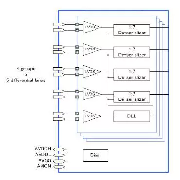
At Silicon Creations, we have developed a power and area optimized, flexible and programmable PMA (Physical Medium Attachment) architecture that can be reliably ported to different process nodes and scaled across protocol generations as data rates increase. It is called the Multi-Protocol PMA, or MP-PMA for short.