The icyflex-V processor is a new ultra-low-power core based on the RISC-V 32-bit ISA, a long-awaited addition to the CSEM icyflex processor family, compatible with off-the-shelf open-source and/or proprietary programming tools. This new development represents a cost effective yet performing alternative to proprietary cores for next-generation ultra-low-power system-on-chip developments. The core was optimized for performance, code density and power consumption and delivers up to 3.2 CoreMark/MHz while consuming as low as 14 uA/MHz in TSMC 55 nm low-power process.
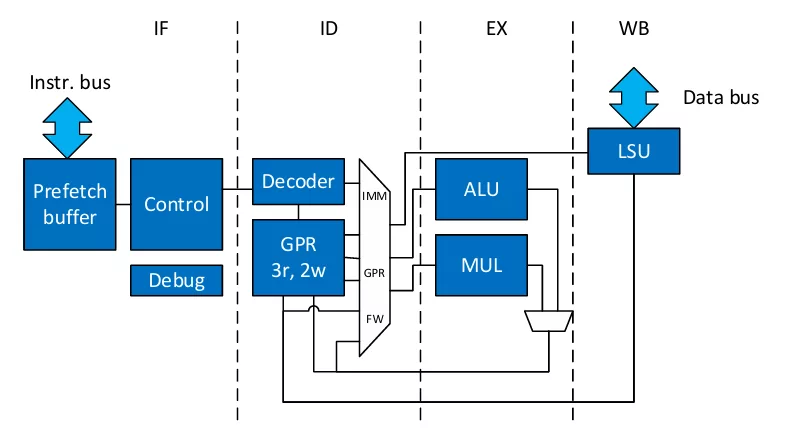
The icyflex-V is a classical 4-stage pipeline (fetch, decode, execute and write-back, Figure 1), implementing the RV32IMC ISA, i.e., a 32-bit integer core supporting the compressed instructions and multiplications. Data forwarding is implemented to avoid pipeline stalls on both ALU outputs and load-store (LSU) outputs caused by read-after-write dependencies. The main target of the core is to be embedded efficiently with a small footprint in ultra-low-power system-on-chip. The main criteria are thus an excellent code density (thanks to compressed instruction) and a limited gate-count achieving good performances. Several options were further taken to reduce the gate-count: the M extension of the ISA is implemented without hardware support for division, which would imply a significant number of gates for a feature not largely used in embedded applications. Similarly, floating-point is left as software emulation to reduce gate-count. In order to achieve state-of-the-art performance though, the 4 stage pipeline was preferred over a 2 stage pipeline that would assuredly be more compact but which would have degraded performances drastically. Similarly, the instruction prefetch buffer implements a simple yet effective branch prediction mechanism that improves the core efficiency at a reasonable gate-count cost.
With these choices, the core achieves a remarkable 3.2 CoreMark/MHz with maximum compiler optimizations, or a 2.8 CoreMark/MHz in balanced performance/code density mode, when using the open-source GCC compiler. The core also reaches a 1.36 DMIPS/MHz. Vendor specific compilers (e.g., IAR) can also be used with the icyflex-V.
Currently, the icyflex-V does not implement non-standard extensions, aiming at keeping a de-facto compatibility with off- the-shelf tools. Specific non-standard extensions might however be added in the future and be used as "intrinsic" assembly instructions to accelerate application specific systems. This could be done seamlessly, without requiring to customize standard compilers.
A debug interface based on the official specification allows to interface the system to on-chip debug tools through a 4-wire JTAG interface. Triggers can optionally be implemented to allow placing breakpoints in flash memories, or to perform data watchpoints. Both open-source software (OpenOCD, GDB, MCU Eclipse) and proprietary tools are supported (Segger Jlink/Embedded Studio, Lauterbach Trace32, IAR Embedded Workbench) by this standard debug interface.
The icyflex-V comes with several peripherals (bus controllers, serial and communication interfaces) that allow customizing systems based on customer requirements. The subsystem can be easily extended with external IP using standard peripheral busses such as APB.
The core is silicon-proven, and an evaluation FPGA-based platform is available. The core is currently being integrated in first customer products and evaluation of its performance in subthreshold libraries is ongoing, paving the way to new ultra low-power records.