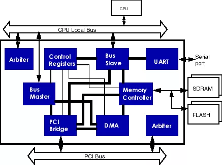
The system controller core connects the system CPU to system memory, PCI bus, IO ports and external communication links. While the CPU’s task in the system is to process data, the system controller’s main function is to coordinate data movement in the system. The system controller contains all the major functional modules required for most System-on-Chip (SOC) application. The entire system controller function can be easily integrated into a single ASIC or PLD.
The system controller contains SDRAM controller, PCI bridge, DMA function, UART, bus arbiter and system control registers. Internal to the system controller, these modules are connected to each other directly to achieve high performance and concurrent data movement between various source and data destinations. Since each module is implemented as synthesizable HDL code, each function can be re-configured or modified as required. All modules are designed with a common interface. The connectivity between the modules can be modified easily to meet different system requirements. Modules not needed for specific application can be removed from the core to minimize die size and gate count.
Different system controllers are available for different CPU types. Currently the CPU supported are: ARM CPU, MIPS CPU with SysAD bus and EC Interface, PowerPC 603, 604, 740, 750, MPC8260, 860, Hitachi SH2, SH3 and SH4. The CPU bus can be 32-bit or 64-bit wide depending on the CPU type. Burst data transfer is supported by the system controller.
CPU Interface
- Different modules to support ARM, MIPS, PowerPC 603, 604, 740, 750, MPC8260, 860, ARM, Hitachi SH2, SH3 and SH4.
- Supports different data sizes as required by the CPU.
- Dispatches CPU request to SDRAM controller, PCI and system registers.
- Provides direct path for CPU to access DMA, UART and optional user-designed logic block.
- Centralized control of all access to system control registers.
- Optionally map PCI target access to system control registers.
- Optional bus master function to access resource on the CPU bus.
Memory Controller
- Allows different modules to access system memory.
- Three request ports to support request from CPU interface, PCI and DMAC.
- Supports industry standard SDRAM and FLASH.
- Programmable memory size and data width.
- Support industry standard 64Mbit, 128Mbit and 256Mbit SDRAMs.
- Supports zero wait state burst data transfer to maximize data bandwidth.
- Programmable SDRAM access timing parameters.
- Automatic refresh generation with programmable refresh intervals.
- Byte collection for FLASH devices with narrow data width.
DMA Module
- Multiple independent DMA channels. Each channel transfer data between SDRAM, PCI and IO ports.
- Burst data transfer optimized for SDRAM access.
- Optimized for single read FIFO in PCI master read to speed up DMA transfer.
- Supports both hardware initiated transfer and software initiated block transfer.
PCI Module
- Operates at different clock domain from CPU bus.
- PCI specification 2.2 compliant.
- Dual FIFO to process master write and target write data transfer.
- Supports data bursting with and without wait states.
- Master receives requests from DMAC and CPU interface.
- Base address registers to map to SDRAM, FLASH, and/or System Register.
- Contains all PCI configuration registers.
- Host bridge generates configuration access to external PCI devices.
- Supports PCI type0 and type1 configuration.
- Arbiter supports 4 or 8 PCI devices.