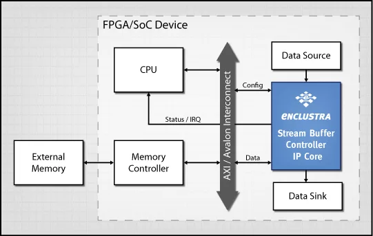
The Stream Buffer Controller IP Core is optimized for Intel (Altera) and Xilinx FPGAs and implements a versatile Stream to Memory Mapped DMA bridge with 16 independent streams. The IP core allows data buffering in an external memory device to provide virtual FIFO capability with up to 4 GB memory size. It provides AMBA® AXI4-Stream interfaces for each write and read data stream. A common memory-mapped master interface (AXI or Avalon) is provided to access the external memory device over an interconnect.
The IP core is highly configurable in terms of operation mode, buffer size and buffer address for each stream. The configuration is done over a memory mapped slave interface, either by an embedded-CPU, by a FPGA Manager application or by an application specific stream configurator controller in VHDL.
Stream Buffer Controller
Overview
Key Features
- Supports up to 16 write and read streams (depending on product options)
- Configurable status flags for write and read path
- Vendor-independent implementation
- Available with Avalon or AMBA-AXI interface
- Data width conversion to/from any byte-multiple width
- The IP Core supports four different operation modes for each channel:
- FIFO mode: writing and reading to the memory is done over the AXI4-Stream interfaces
- Write mode: Writing to the memory is done over the AXI4-Stream, Reading from the memory is done by a CPU.
- Read mode: Writing to the memory is done by a CPU, reading from the memory is done over the AXI4-Stream interface.
- ROM mode: Reading from the memory is done over the AXI4-Stream interface. The memory must be initially written by a CPU
Benefits
- Supports data width conversion for the write and read data streams
- The use of different operation modes provides the implementation of versatile applications with a single IP core.
- Easy integration thanks to the unified bus interface and the clearly laid out register bank
- A stand-alone solution without the need of a CPU can be easily realized by a stream configuration controller that is provided in VHDL
Block Diagram
Applications
- Data acquisition
- Image processing
- Test and measurement
- Embedded processing
Deliverables
- Stream Buffer Controller IP Core
- VHDL source files (plain or encrypted, depending on product options)
- Reference design
- User manual
- Stream Buffer Controller API
- C source code
- Application software example
- User manual
- Stream Buffer Controller IP core reference design
- Reference design top-level VHDL file (plain VHDL)
- UCF / XDC / SDC constraint files (depending on product options)
- Xilinx® ISE / Xilinx Vivado™ / Intel® Quartus® project files (depending on product options)
- Top-level simulation test bench file (plain VHDL)
- Top-level simulation ModelSim project file
- Documentation
Technical Specifications
Maturity
IN BETA PHASE
Related IPs
- Stream Buffer Controller
- SSTL2 Buffer (Vcc=2.5V,Vcore=1.25V, Freq=800Mbps)
- HSTL Buffer (Vcc/Vdd=3.3V/1.8V,Vref=0.75V, Input Swing:0.65~0.85V, Freq=600Mbps)
- SSTL2 Buffer (Vcc=2.5V,Vcore=1.25V, Freq=800MHz)
- HSTL Buffer (Vcc/Vdd=3.3V/1.8V,Vref=0.75V, Input Swing:0.65~0.85V, Freq=600Mbps)
- InGaP HBT low power buffer amplifier