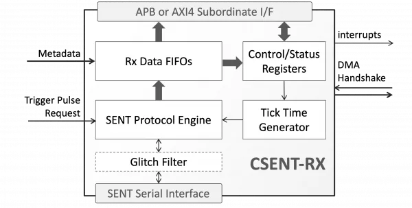
Learn more about SENT IP core
The JESD204 Transport Layer oversees converter data mapping onto a set of JESD204 Lanes. The nature of these lanes is dependent on the version of the JESD204 standard and a function of the PCS and over the years despite the Serdes technology changing with ever increasing line rates, the function and features of the Transport Layer remained the same
Integrating PQC into a widely deployed IKEv2 implementation is an important step toward making secure communication future-proof. We integrated ML-KEM, the NIST-standardized module-lattice KEM, into StrongSwan’s IKEv2 stack using our own KiviPQC-KEM hardware accelerator.
In a computer system, both the GPU as well as the monitor have a certain rate at which they render or update an image, respectively. The rate is nothing but the frequency at which the image is refreshed (updated in the image it shows/displays), usually expressed in hertz, and can vary based on the content displayed on the screen.
Explore verification challenges that arise when dynamically resizing links during runtime. These challenges are especially relevant in AI, HPC, automotive, and mobile SoC applications that demand aggressive power
Morgan State University (MSU) recently received an Apple Innovation Grant, designed to support engineering schools as they develop their silicon and hardware technologies. The New Silicon Initiative (NSI) is designed to inspire and prepare students for careers in hardware engineering, computer architecture, and silicon chip design.
The Ultra Ethernet Consortium is introducing a link-layer retry mechanism to avoid costly recovery at higher layers.